When people talk about printed circuit boards, beginners often mix up the terms “PCB schematic” and “PCB design file.” They point to different things. Knowing the difference is key to making a PCB that works. Below, a Shenzhen PCBA company explains the difference between a PCB schematic and a PCB design file.
What is a PCB?
Before we look at the differences between a schematic and a design file, we need to know what a PCB is.
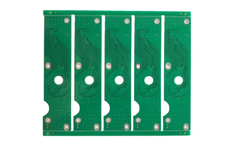
A PCB, or printed circuit board, is the board inside most electronic devices. It is a flat board that holds parts and links them with copper tracks. The board lets parts work together so the device runs. Without a PCB, most electronic devices would not work.
What is a PCB schematic and what is a PCB design file?
A PCB schematic is a simple two-dimensional map of an electrical circuit. It shows how parts work together and how they connect. A schematic uses standard symbols to show parts and connections. The schematic tells which parts will be used and how each part will link to others.
A PCB design file is the layout, or the physical view, of the board. It shows where the parts will sit on the board after the circuit works as planned. The design file includes copper traces and holes. It shows the exact place for each part and how each part is tied to the copper.
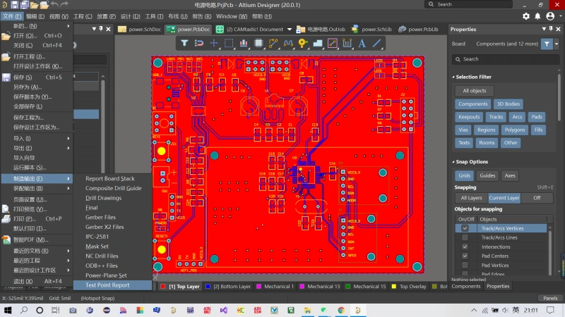
In short, the schematic is the plan. It is the blueprint for the circuit. It shows how the circuit will be connected, but not the exact places where parts will sit. The design file is the physical plan. It takes the schematic and turns it into a board layout that can be made.
The schematic is the first step in the design process. It is a drawing or a data file that uses agreed symbols. Anyone who reads the schematic should see how the circuit works. The design file is the next step. It uses the schematic to lay out the board in two or three dimensions. The design file is used to build the real board that will be tested. Once both steps are done and the board works as expected, the manufacturer can make the PCB.
Parts of a PCB schematic
Now that we know the main difference, we will look closer at the parts of a PCB schematic. As we said, the schematic shows all of the connections, but you should keep a few points in mind:
- The schematic is not made to scale so the connections may look far apart. In the actual layout the parts may sit close to each other.
- Some lines may cross in the schematic. In the real board those crossings are not possible unless they are on different layers or use vias.
- Some linked parts may sit on the opposite side of the layout. The schematic will show a label to say they are connected.
- A full schematic can take one page, two pages, or many pages to show every part of a design.
- For a complex circuit you can group parts by function. This makes the schematic easier to read. The layout stage will not keep the same arrangement, so the schematic often looks different from the final 3D board.
Key elements you will find in a PCB schematic
- Symbols for parts:Each part has a symbol. Resistors, capacitors, diodes, transistors, connectors, switches, and ICs all have standard symbols. The symbol shows the part function and how it connects.
- Part names and values:Parts have a reference name (for example R1, C2, U3). They also have a value or part type. The schematic shows these so builders know which part to use.
- Net names and wires:Wires are lines that link parts in the schematic. Nets are names for wires that carry a signal or power. Net names help show that two points are the same net even if they are not on the same page.
- Power and ground symbols:Power rails and ground are shown with clear symbols. These show which parts get power and how the board is powered.
- Notes and test pointsSchematics can include notes for assembly and test points for debugging. Test points help engineers measure voltages and signals during testing.
- Connectors and pin maps:Connectors and their pin layout are shown in the schematic. The pin map shows which wire goes to which pin on a connector.
- Reference to the BOM:The schematic links to the bill of materials (BOM). The BOM lists the exact parts, part numbers, and any supplier info.
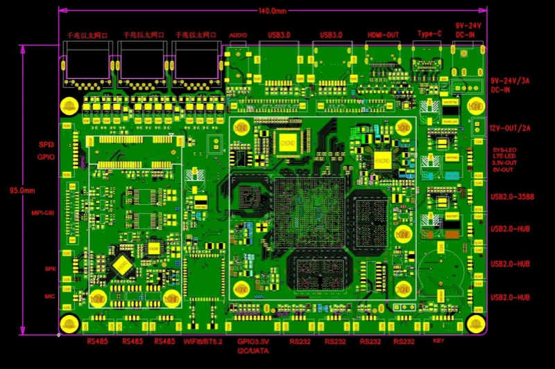
What is in a PCB design file?
The PCB design file is the physical plan for the board. It moves from the schematic view to the board view. The file is what the board house uses to make the PCB. It contains many layers and details.
Main parts of a PCB design file
- Board outline:The board outline sets the exact shape and size of the PCB. It is the edge where the board will be cut. The outline also shows mounting holes and cutouts.
- Component placement:The design file shows the exact place for each part on the board. The part footprints show where the pins, pads, and body go. The placement must allow for soldering, testing, and heat flow.
- Copper layers and traces:The traces are the copper lines that link pads and vias. A design file can have one, two, or many copper layers. The file shows trace width, spacing, and routing on each layer.
- Vias and holes:Vias are holes that let traces move from one layer to another. The design file sets via size and location. It also sets plated through holes for through-hole parts.
- Drill fileThe drill file lists the holes that the board must have. This includes via holes and mounting holes. The board house uses this file to drill the right holes.
- Solder mask and paste mask:The solder mask layer defines where the board will keep copper exposed for soldering. The paste mask defines where solder paste will go for SMD parts. These layers are part of the design file.
- Silkscreen or legend:The silkscreen layer has labels, part outlines, and text on the board. The silkscreen helps assembly and repair by marking part IDs and orientation.
- Mechanical and assembly layers:These layers show mechanical details and assembly notes. They can include keepout zones, mounting guides, and special assembly marks.
- Layer stack and thicknessFor multi-layer boards, the file includes a stackup. The stackup shows the order of layers and the thickness of each layer. The stackup is important for impedance control and mechanical strength.
How the schematic and design file differ in practice
The schematic shows the electricity and the idea. The design file shows the real board and the place for each part. The schematic is about function and link. The design file is about space and form. The schematic is for anyone to read and to know how the circuit works. The design file is for the board maker and for testing the real board.
When you move from schematic to design, you must check many things:
- Part size and footprint are correct.
- Pins and pads match the schematic symbols.
- All nets in the schematic are present in the layout.
- No two traces end up crossing on the same layer. If they do, change routing or add vias.
- Clearance rules and trace widths meet current and heat needs.
- Thermal issues and placement for heat-generating parts are handled.
- Connectors and edges fit the mechanical design.
Performance and the design file
The design file is where performance matters more. The engineer builds the real board from the design file to test the device. The layout affects how the board will work. The layout also must follow the physical needs of the board.
Some real design checks include:
- How close parts are for heat spread and cooling.
- Where the connectors sit on the board edge.
- How wide traces must be to carry the needed current.
- Where vias and planes sit for good ground and power distribution.
The silkscreen layer also appears in the design file. The silkscreen shows letters, numbers, and symbols that help assembly and use. The silkscreen helps the board house place parts in the right place.
If the board does not work after assembly, the design must be redrawn. The design file is not the final step until the built board passes test. If the board fails, the engineer returns to the schematic or layout to change the design.
Why people mix them up
People mix up the schematic and the design file because both are part of the board design. They are linked, and they both are needed to make the PCB. But they are different stages in the process. The schematic comes first. The design file comes next.
Steps to make sure both are right
- Start with a clear schematic.
- Choose correct footprints for each part.
- Link the schematic nets to the layout nets.
- Run a design rule check (DRC) to find errors.
- Make a drill file and Gerber files for manufacturing.
- Check the stackup and trace widths for the needed current and signal integrity.
- Test the first prototype and then change the design as needed.
Заключение
Although PCB schematics and PCB design files are often confused, they are separate steps in making a printed circuit board. The schematic is the electrical map that shows how parts link. The design file is the physical layout that shows where parts sit and how copper traces run.
First make the schematic so you have a clear plan. Then make the design file so you can build the board and test it. When both are correct, the PCB can be manufactured and will work as planned.