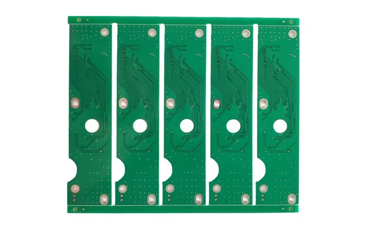
The main purpose of baking PCBs is to remove moisture. This means getting rid of water that is inside the PCB or that the PCB has absorbed from the air. Some PCB materials attract water easily. That water can cause big problems later.
After production, PCBs can pick up moisture from the environment while they sit in storage. Water is one of the main causes of popcorn and delamination in PCBs. Popcorn means the board can blister or even split open when heated. Delamination means the layers of the board partly or fully separate.
When a PCB is heated above about 100°C, for example in a reflow oven, a wave solder oven, during hot-air leveling, or during hand soldering, water turns to vapor. The vapor expands fast. If the vapor expands faster than it can escape from the board, it can push the layers apart or break internal structures.
If the board is heated faster, the vapor expands more quickly. If the temperature is higher, the vapor volume is larger. If the vapor cannot escape, it can blow up the PCB.
The board is weakest in the Z direction. Vapor pressure can break through vias that connect layers. Vapor can also separate layers. In severe cases, the outer surface of the board can bubble, bulge, or crack open. Sometimes the damage is not visible on the surface. But the board can have internal damage. Later this can cause product instability, conductive anodic filament (CAF), or other failures. The product can fail in the field.
Root causes of PCB popcorn and delamination and how to prevent them
Baking PCBs is not simple. You must remove the original packaging before you put the board into the oven. You must heat the board above 100°C. But the temperature must not be too high. If the board heats too fast, trapped water can expand too quickly and damage the board.
In industry, many use 120 ± 5°C as a baking temperature. This helps ensure moisture is removed before the board goes to SMT and reflow. Baking time depends on board thickness and size. Thin boards and very large boards may need special handling after baking. After baking, these boards should be pressed with a heavy flat plate to avoid warping during cooling. Warped boards cause problems in later steps.
If the PCB warps, solder paste printing can be off. This leads to uneven paste thickness and misalignment. In reflow, this can cause many shorts or many poor solder joints.
Typical baking rules and time settings
Below are common rules used in the industry. These are based on age since manufacturing and on storage conditions.
- If the PCB is within two months from the manufacturing date and was sealed well, and after unpacking it was stored under controlled temperature and humidity (≤ 30°C / 60% RH, per IPC-1601) for more than five days, bake at 120 ± 5°C for 1 hour before use.
- If the PCB was stored between 2 and 6 months from the manufacturing date, bake at 120 ± 5°C for 2 hours before use.
- If the PCB was stored between 6 and 12 months from the manufacturing date, bake at 120 ± 5°C for 4 hours before use.
- If the PCB was stored over 12 months, do not use it if possible. The adhesive in multilayer boards weakens with time. Old boards can cause unstable product performance and more field repairs. Also old boards have a higher risk of popping or poor solderability during production. If you must use boards stored over 12 months, bake at 120 ± 5°C for 6 hours first. Before mass production, do a trial print and a few boards to check solderability and reliability.
Another reason to avoid old PCBs is surface finish aging. For ENIG (electroless nickel immersion gold), industry shelf life is generally 12 months. After that, if the gold layer is thin, nickel can diffuse and appear at the gold surface. This can form oxides and hurt reliability. Be careful.
- Use all baked PCBs within 5 days. If not used up, vacuum pack them again. If a board was baked but not used and stayed exposed, re-bake at 120 ± 5°C for 1 hour before use.
How to stack PCBs in the oven
Correct stacking helps good heat flow and prevents warping.
- For large PCBs: lay them flat in stacks. One stack should not exceed 30 boards. After baking, open the oven within 10 minutes and remove the boards. Lay them flat to cool. After cooling, press them with an anti-warp fixture. Do not bake large boards standing on edge. Standing can cause board bowing.
- For medium and small PCBs: you can stack them flat, up to 40 boards per stack. You can also bake them standing on edge. When baking finishes, open the oven within 10 minutes and remove boards. Lay them flat to cool. After cooling, press with an anti-warp fixture.
Important precautions during baking
- Do not bake at a temperature above the PCB Tg. Generally do not exceed 125°C. Older leaded PCBs often have lower Tg. Most modern lead-free PCBs have Tg above 150°C.
- Use baked boards quickly. If they are not used, vacuum pack them again. If they stay in the shop too long, re-bake.
- The oven should have an exhaust or a fan for drying. If not, the vapor can stay in the oven and increase its humidity. That reduces bake effectiveness.
- From a quality view, fresher PCBs give better results after reflow. Even if you bake older boards, there is still a higher quality risk.
Practical baking suggestions
- Some recommend baking at 105 ± 5°C. Water boils at 100°C. If you go over the boiling point, water will turn to vapor. The amount of water inside a PCB is usually small. So you do not need very high temperature to speed up vaporization.
High temperature or very fast vaporization can cause vapor to expand quickly. That can harm the board. For multilayer boards and buried vias, 105°C is just above water boiling point. This is high enough to remove moisture and low enough to cut oxidation risk. Modern ovens also control temperature better than older ovens.
- Decide if baking is necessary by checking the vacuum pack. Look at the packaging’s Humidity Indicator Card (HIC). If the HIC shows no moisture, and the packaging is good, you may run the board directly without baking.
- For baking, standing boards on edge with spacing is often best. This allows better air flow and heat convection. The trapped moisture vents out more easily. For very large boards, check if standing will cause warping. If warping risk is high, bake flat.
- After baking, store boards in a dry place and cool them quickly. Put an anti-warp fixture on top of the stack while cooling. Objects usually absorb moisture when they cool slowly. But fast cooling can cause warpage. Find a balance.
Disadvantages and trade-offs of baking
- Baking speeds up oxidation of the board surface. Higher temperature and longer bake time make oxidation worse.
- Do not bake OSP (organic solderability preservative) boards at high temperature. OSP film can degrade at high heat. If you must bake OSP boards, use 105 ± 5°C and do not bake more than 2 hours. After baking, use the boards within 24 hours.
- Baking can affect IMC (intermetallic compound) growth for surface finishes like HASL (hot air solder leveling) or ImSn (immersion tin). IMC forms between copper and tin or other metals during earlier steps. Baking can increase the thickness of already formed IMC. Thicker IMC can hurt reliability.
Notes on surface finishes and storage life
- ENIG: shelf life about 12 months. After that, nickel diffusion and oxidation can appear if gold is thin.
- HASL and ImSn: these finishes already have IMC formed in prior steps. Baking may cause IMC to grow thicker. Thicker IMC can make soldering less reliable.
- OSP: film can fail at high temperature. Avoid high temperature and long bake times.
Final practical checklist
- Check vacuum bag and HIC first. If HIC shows dry and storage was good, no bake may be needed.
- If you need to bake, follow recommended times based on storage age. Use 120 ± 5°C as a common industry setting. For conservative approach, 105 ± 5°C can work and reduce oxidation risk, especially for OSP and sensitive boards.
- Do not exceed the PCB’s Tg. Know the Tg of the board material. Most lead-free boards have Tg > 150°C. Old leaded boards may have lower Tg.
- Use a drying oven with an exhaust fan. This keeps oven humidity low.
- Stack boards correctly. For large boards, flat stack, max 30. For medium/small, flat stack max 40 or stand them.
- Remove boards from oven within 10 minutes after bake. Lay them flat to cool and press with anti-warp fixture.
- Use baked PCBs within 5 days. If not used, re-vacuum pack or re-bake.
- For OSP, limit bake to 105 ± 5°C and less than 2 hours. Use within 24 hours.
- For boards stored over 12 months, avoid use. If forced, bake long (120 ± 5°C for 6 hours) and run trial production to confirm solderability.
- Before mass production, run tests: solderability test, print trial, and reflow samples. Confirm no solderability issues or reliability risks.
Summary
Moisture in PCBs is a real risk. It can cause popcorn, delamination, via break, and hidden internal damage that leads to field failures. Baking removes moisture but it is a process with trade-offs. Overbaking or too-high temperature can cause oxidation, damage finishes like OSP, and change IMC thickness. Use simple rules: check HIC and packaging, use controlled oven with exhaust, do not exceed Tg, follow time rules based on storage age, stack and cool boards properly, and test before mass run. These steps help prevent reflow failures and improve product reliability.