Introduction: The Foundation of Flexible Electronics
In an era defined by compact, high-performance electronics, the humble circuit board has evolved dramatically. Flexible and rigid-flex PCBs are no longer niche components but the backbone of modern innovation, from wearables to aerospace systems. The success of these advanced PCB designs hinges on a foundational, yet often overlooked, element: the stackup and layer order. A well-designed stackup is the blueprint for electrical performance, mechanical durability, and manufacturing success.
Why Flexible PCB Stackup and Layer Order Design Matters
The stackup—the arrangement of copper and dielectric layers—is not merely a list of materials; it dictates the entire character of the circuit board. It governs critical electrical properties like signal integrity and impedance control, while also defining mechanical characteristics such as bend radius and long-term reliability. A poor stackup can lead to signal degradation, EMI issues, and premature mechanical failure. For flexible circuits, where weight and volume are paramount, a thoughtful stack-up design can achieve substantial savings; flexible PCBs can reduce volume by up to 60% and weight by up to 70% compared to their rigid counterparts.
Scope of This Guide: From Fundamentals to Advanced Strategies
This guide provides a comprehensive overview of flexible and rigid-flex PCB stackup design. We will deconstruct the fundamental materials and their properties, explore core principles of layer ordering, and delve into advanced strategies for optimizing performance and ensuring manufacturability. Whether you are designing a simple single-layer flex circuit or a complex multi-layer rigid-flex PCB, mastering these concepts is essential.
Understanding Flexible PCB Stackup Fundamentals
Before diving into complex designs, it’s crucial to grasp the basic structure and purpose of a flexible PCB stack-up. This foundation informs every subsequent design decision.
Defining the Flex PCB Stack-Up
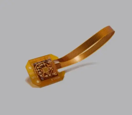
A Flex PCB stack-up is the detailed arrangement of all the layers that constitute the flexible circuit. It specifies the sequence, thickness, and material type for each conductive copper layer and insulating dielectric layer. This blueprint is created before layout begins and is a critical document for both the designer and the manufacturing partner, ensuring the final product meets all electrical and mechanical specifications.
Types of Flexible PCBs and Their Basic Stack-Ups
Flexible circuits are categorized by their layer count, with each type having a typical stack-up:
- Single-Sided Flex: The simplest form, consisting of a single copper layer on a polyimide dielectric base, protected by a coverlay. Ideal for “bend-to-install” applications.
- Double-Sided Flex: Features a copper layer on both sides of the core dielectric layer, interconnected with plated through-hole vias. This allows for denser circuit routing.
- Multi-Layer Flex: Contains three or more conductive layers separated by dielectric material. These complex structures support high-density components and sophisticated routing but require careful design to maintain flexibility.
Deep Dive into Flexible PCB Materials and Their Properties
The choice of materials is the most critical factor in stackup design. Each material plays a distinct role in the circuit’s overall performance, durability, and cost.
Copper Layers: The Electrical Backbone
Copper serves as the conductive pathway in a flexible circuit. The two primary types used are:
- Rolled-Annealed (RA) Copper: This type has a smooth surface and an elongated grain structure, making it highly flexible and resistant to fatigue from repeated bending. It is the preferred choice for dynamic flex applications.
- Electro-Deposited (ED) Copper: ED copper has a rougher vertical grain structure. While less flexible than RA copper, it offers better adhesion and is a cost-effective option for static flex applications where the board is only bent during assembly.
Dielectric Materials: Insulation and Performance
The dielectric core provides insulation between copper layers and is the primary source of the board’s flexibility.
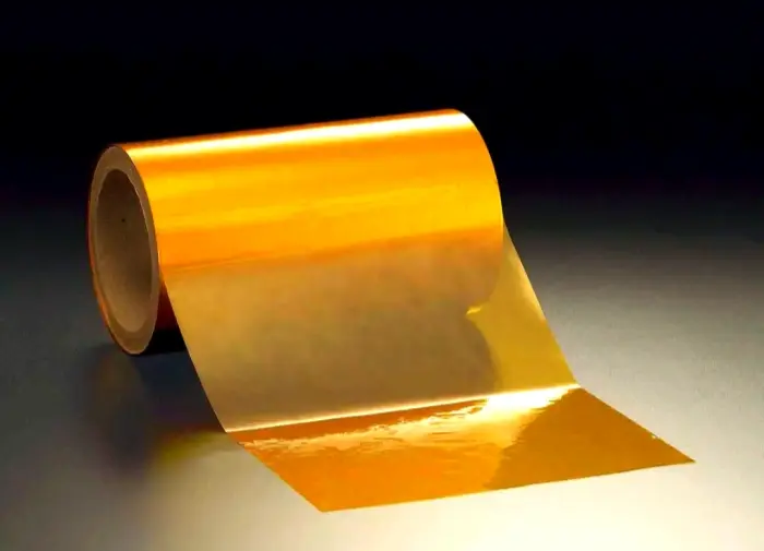
- Polyimide (PI): This is the industry-standard material for flexible PCBs due to its excellent thermal stability, chemical resistance, and superior mechanical properties. Its dielectric constant (Dk) is a key factor in controlled impedance calculations.
- Adhesiveless vs. Adhesive-based Cores: Adhesiveless cores, where copper is directly bonded to the polyimide, are thinner and more flexible, making them ideal for high-performance and dynamic applications. Adhesive-based cores use a layer of acrylic or epoxy to bond the copper, which is more economical but slightly thicker and less flexible.
Adhesives: Bonding the Layers
Adhesives are used to bond the coverlay to the core or, in rigid-flex PCB designs, to laminate different layers together. Acrylic and epoxy are common choices, selected based on thermal performance and bonding strength requirements. In rigid-flex manufacturing, “no-flow” pre-pregs are often used to bond rigid sections without adhesive seeping into the flexible areas.
Coverlays & Soldermask: Protection and Definition
- Coverlay: A sheet of polyimide with an adhesive backing laminated onto the outer copper layers. It serves as the flexible equivalent of a soldermask, providing electrical insulation and protection from environmental factors like moisture and abrasion.
- Soldermask: In rigid sections of a rigid-flex PCB, a traditional liquid photoimageable (LPI) soldermask is used to define solder pads and protect traces.
Stiffeners: Localized Support and Component Mounting
Stiffeners are rigid materials applied to specific areas of a flex circuit to provide localized support. They do not have an electrical function. Common materials include Polyimide, FR-4, or metal. A stiffener is essential for supporting components and connectors, preventing stress at solder joints, and ensuring a flat surface for ZIF connector mating.
Core Principles of Layer Order and Stackup Design
A logical and symmetrical layer order is fundamental to creating a reliable and high-performing flexible circuit board.
Determining Optimal Layer Counts
The number of layers is driven by circuit density, signal routing requirements, and impedance control needs. While adding layers provides more routing space, it also increases thickness, reduces flexibility, and raises costs. The goal is to use the minimum number of layers necessary to meet all design requirements.
General Layer Ordering Guidelines
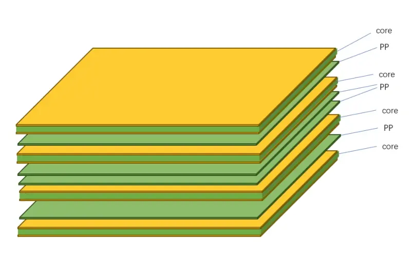
- Symmetry: A symmetrical stack-up, balanced around the center of the board, is crucial. It prevents warping and bowing during manufacturing and thermal cycling.
- Neutral Bend Axis: For dynamic applications, place conductive layers as close to the center (the neutral bend axis) as possible. This minimizes tensile and compressive stress on the copper during bending, significantly improving fatigue life.
- Layer Orientation: In multi-layer flex, orient traces on adjacent layers perpendicularly (e.g., top layer horizontal, next layer vertical) to improve structural integrity and reduce crosstalk.
Power and Ground Planes in Flex Design
Solid ground and power planes are essential for good signal integrity, providing a stable voltage reference and a clear return path for high-speed signals. In flexible designs, a cross-hatched pattern for these planes is often used instead of solid copper. This maintains electrical connectivity while significantly increasing the board’s flexibility.
Signal Layers and Routing Considerations
High-speed signal traces should be routed on internal layers, sandwiched between ground or power planes. This configuration, known as a stripline, provides excellent shielding against electromagnetic interference (EMI) and helps maintain consistent impedance. Outer layers (microstrip) are more susceptible to noise.
Stackup of FPC with Airgap Thickness
In multi-layer flexible circuits requiring high flexibility, an “air-gap” construction is often used. Instead of bonding all layers together, selective bonding is applied, creating separate, unconnected flex layers in the bending zone. This dramatically improves flexibility by allowing the layers to move independently, much like the pages of a book.
Critical Design Considerations for Performance and Reliability
Beyond materials and layer order, several design factors directly influenced by the stackup are critical for ensuring the final product works as intended.
Bend Radius and Dynamic Bending
The minimum bend radius a flex circuit can tolerate is directly proportional to its thickness. A thicker stack-up requires a larger bend radius to avoid damaging the copper traces. For dynamic applications with continuous flexing, a single-layer or adhesiveless double-layer stack-up is strongly preferred to maximize fatigue life.
Controlled Impedance Design
For high-speed electronics, maintaining a specific impedance (typically 50 ohms) is vital for signal integrity. Impedance is controlled by the trace width, the dielectric material’s thickness, and its dielectric constant (Dk). The stack-up defines these parameters, making it the foundation of any controlled impedance design.
Signal Integrity (SI) and Electromagnetic Interference (EMI)
A well-designed stack-up is the first line of defense against SI and EMI issues. Properly placed ground planes provide a low-inductance return path, minimizing signal reflections and noise. Shielding sensitive signal layers between ground planes effectively contains electromagnetic fields, preventing crosstalk and reducing emissions.
Thermal Management in Flexible PCBs
Polyimide has a lower thermal conductivity than FR-4. Heat generated by components must be managed effectively to prevent damage. The stack-up can aid in this by incorporating thicker copper layers or planes to help spread heat. In some designs, metal stiffeners or dedicated heat sinks can be bonded to the flex circuit.
Mechanical Robustness and Strain Relief
The transition from a rigid area to a flexible one in a rigid-flex PCB is a point of high mechanical stress. The stack-up design must ensure a smooth transition. Extending the coverlay over the edge of the stiffener and using gradual width transitions for traces can significantly improve durability.
Via Specifications and Placement
Vias create electrical connections between layers but also introduce mechanical stiffness and potential failure points. In flexible areas, vias should be avoided in or near bend zones. When necessary, they should be well-supported and designed with tear-dropping to reduce stress concentration at the pad-to-trace interface.
Rigid-Flex PCB Stackup: Bridging the Gap
Rigid-flex PCB designs introduce unique challenges by combining two distinct manufacturing technologies into one seamless component.
Unique Challenges of Rigid-Flex Stackup
The primary challenge is managing the different material sets and thicknesses between the rigid and flexible sections. The flexible polyimide core typically runs through the entire board, while layers of FR-4 and pre-preg are selectively added to form the rigid sections. This complex lamination process requires precise control to ensure proper bonding and avoid defects.
Designing the Critical Transition Zones
The interface where the rigid section ends and the flexible section begins is the most critical area. The stackup must be designed to manage stress effectively. This includes staggering the termination points of the rigid layers and ensuring the coverlay from the flex section extends slightly underneath the rigid portion to act as a strain relief, preventing delamination and trace cracking.
Conclusion
The design of a flexible or rigid-flex PCB stackup is a meticulous balancing act between electrical requirements, mechanical constraints, and manufacturing realities. It is far more than a simple list of materials; it is the strategic foundation upon which the entire performance and reliability of the final electronics product is built. By carefully selecting materials like polyimide and RA copper, establishing a symmetrical and logical layer order, and considering critical factors like signal integrity, bend radius, and the unique challenges of rigid-flex transition zones, designers can unlock the full potential of flexible circuit technology. A well-planned stack-up, developed in collaboration with your manufacturing partner, is the first and most crucial step toward a successful and robust flexible PCB design.