Intro
Demand for small, high-density, multi-function, high-performance electronics is rising. Good soldering is key for PCBA quality. If soldering is poor, the product can fail. In this article we list the main factors that affect SMT soldering quality. We also give simple, practical fixes we use in production. Sentences are short and clear. Words are simple.
Why SMT soldering matters
SMT soldering links parts to the PCB. Good soldering makes the circuit work. Bad soldering causes failures. If soldering is not checked, even a good design can fail. We inspect solder joints and the area around them. We check wires, terminals, and hooks for damage or dirt. Many electrical failures come from bad soldering.
Where soldering defects appear
Solder defects often show up in the reflow stage. But reflow is not the only cause. Solder quality depends on many things. These include:
- BOM and component quality.
- PCB pad design and manufacturability.
- Solder paste type and condition.
- Stencil design and printing process.
- Placement accuracy and machine settings.
- Reflow profile and oven condition.
- Worker skill and process control.
If one link fails, the final solder can fail. We check each step.
BOM preparation — why it matters and what we do
BOM quality links directly to reflow quality. We check:
- Component packaging must suit automatic pick-and-place.
- Part shapes must meet SMT size and tolerance rules.
- Solderable ends on parts and PCB pads must be clean and not oxidized.
If parts or pads are oxidized or damp, we see defects like poor wetting, cold joints, solder balls, and voids. Moisture is a big risk. We store moisture-sensitive parts in dry boxes. We bake parts before use when needed.
Fixes we use
- Confirm BOM vs. component specs before production.
- Store MSL parts in dry cabinets.
- Bake parts per manufacturer rules before placement.
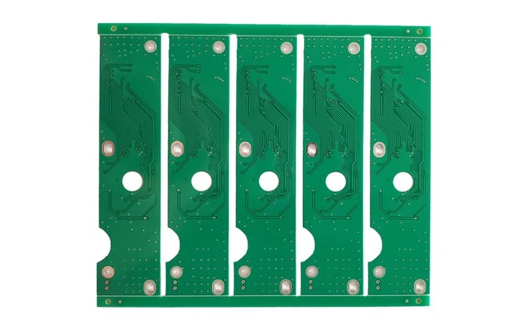
PCB pad design and manufacturability
PCB design is the top factor for SMT success. Poor pad design causes many defects. We follow these points:
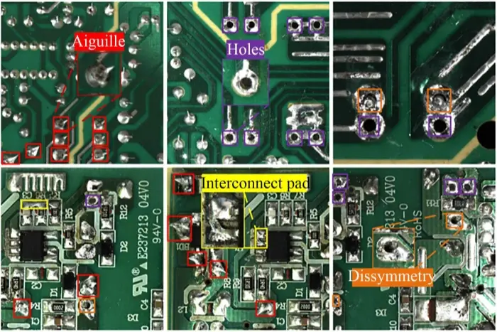
- Pad symmetry. For small chips (0805 and below) make pad ends symmetric. This balances molten solder forces. If one side has much more copper, use a thin trace to connect large copper areas.
- Pad spacing. Too small or too large spacing causes poor fillet or bridging.
- Pad size. Ensure enough pad area for a proper solder fillet.
- Pad width. Match pad width to component terminal width.
- No through-holes on pads. Through holes in pads pull solder away during reflow. This can cause cold joints and shorts.
Fixes we use
- Review PCB with DFM checklist before fabrication.
- Use IPC pad guidelines for common packages.
- Ask PCB vendor for sample pads or panel proofs for new designs.
Solder paste printing — key points and fixes
Solder paste printing causes most rework when PCB design is correct. Printing needs three things: paste, stencil, and squeegee.
Paste quality
Solder paste mixes alloy powder and flux. Alloy percentage is 80–90% by weight. Flux removes oxidation and helps wetting. Store paste at 0–10°C or per maker specs. Use paste within shelf life. Keep factory at ~25°C and 50% humidity if possible. Let paste rest and stir before use. After printing, reflow within 2 hours or follow paste rules.
Fixes
- Follow paste storage and handling rules.
- Keep workshop temp and humidity stable.
- Mix paste well before printing.
Stencil design and manufacturing
Stencil deposits paste on pads. Bad stencils cause bad prints. Stencils are made by chemical etch, laser, or electroform. We check:
- Stencil thickness set by smallest pitch.
- Aperture shape and smooth walls.
- Area ratio for tiny parts (0201, BGA).
- Anti-wick (OHP) patterns for large pads to avoid excess solder.
- Marks for alignment.
- Proper print direction to avoid bridges.
Fixes
- Use electroformed stencils for fine pitch when needed.
- Use area ratio and trapezoid apertures for small parts.
- Add fiducials on stencil matching PCB.
Squeegee and print parameters
Squeegee type, angle, speed, and pressure matter. Wrong settings cause too much or too little paste.
Fixes
- Use nickel-plated steel squeegee, ~60° angle typical.
- For through-hole components, use 45° to add more paste.
- Tune speed and pressure. Slow speed often gives better print, but not too slow.
- Clean stencil often and choose correct cleaning mode.
Equipment accuracy and PCB support
Printer accuracy and board support matter. Poor support or bent PCB leads to uneven prints.
Fixes
- Use stable, flat PCB supports.
- Maintain printer calibration.
- Check repeatability for high-density boards.
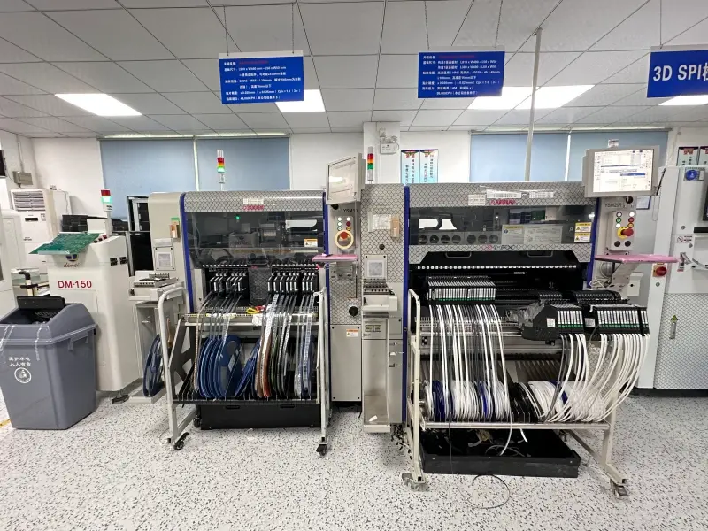
Component placement — errors and solutions
Good placement needs correct parts, precise coordinates, and proper nozzle pressure.
- Use correct parts that match BOM.
- Check orientation and polarity.
- Set pick-and-place pressure and Z height right.
- Keep accurate feeders and nozzles.
Fixes
- Run placement tests for new boards.
- Use vision systems and fiducials for alignment.
- Train operators on feeder setup and nozzle care.
Reflow soldering — profile and control
Solder joints depend on the reflow temperature profile. A good profile gives full wetting and good fillets. Bad profiles cause tombstoning, solder balls, and poor joints.
Key points:
- Peak temp usually 30–40°C above paste melting point.
- Avoid heating too fast. Too fast can damage parts and PCB.
- Avoid too high peak or long dwell. That can damage heat-sensitive parts.
- Use nitrogen reflow for high quality and less oxidation if needed.
Set profile based on:
- Paste manufacturer recommended curve.
- Component thermal limits.
- PCB material, size, and mass.
- Reflow oven type and zone lengths.
Fixes
- Profile the board with thermocouples.
- Adjust conveyor speed and zone temps.
- Use nitrogen when required.
Final inspection and test
After reflow we inspect visually and electrically. Visual checks look for fillet shape, bridging, cold joints, and solder balls. We inspect surrounding areas for solder splashes and pads damage. Many component failures found in electrical tests come from bad soldering.
Fixes
- Use AOI and X-ray for hidden joints and BGAs.
- Perform in-circuit tests or flying probe tests.
- Log defects and trace back to the process step.
Main takeaways — what matters most
Many factors affect SMT soldering quality. The most critical are:
- Component, PCB, and paste quality. If these fail, fixes are hard.
- Good PCB pad design. This prevents many defects.
- Stable and correct solder paste printing. Many reworks come from print errors.
- Proper reflow profile and machine maintenance.
- Skilled operators and strict process control.
We believe the first step is strong material control and good PCB pad design. Then control paste printing and reflow. Finally, train staff and run tests.