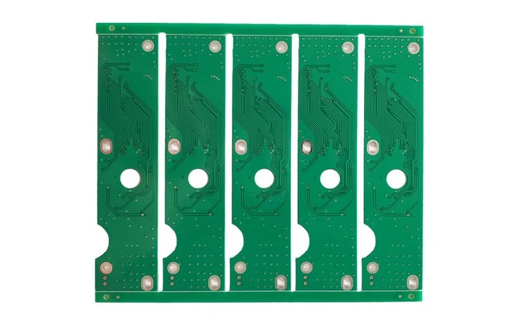
When our clients design printed circuit boards, they often face the challenge of optimising costs while maintaining reliable electrical performance. Copper thickness directly influences both the price and function of every PCB. By making informed decisions, you can avoid unnecessary expenses while ensuring reliable performance.
Copper Thickness and PCB Cost
Increasing copper thickness will increase PCB costs from both material and manufacturing process perspectives.
Material Costs and Manufacturing Challenges
As a primary raw material, the amount of copper used directly determines the substrate cost of a PCB. As the board size or layer count increases, thicker copper layers consume significantly more raw material. For instance, in multilayer heavy copper designs, copper usage multiplies rapidly.
Transitioning from standard to heavy copper yields a significant cost jump. Comparing the cost of 1 oz vs. 3 oz copper reveals this clearly: 1 oz copper costs approximately $0.50 per square foot, while the cost for 3 oz copper rises to around $1.50. In practical production, increasing copper thickness from 1 oz to 3 oz can increase the total board cost by 30% to 50%, depending on design complexity and the manufacturer. The cost per additional ounce of copper rises at a steeper rate due to the added material, more complex processing, and stricter quality controls required.
Selecting thicker copper not only increases material expenses but also introduces a series of challenges in fabrication and processing. These process challenges translate directly into higher production costs:
| Challenge | Description |
| Drilling | Thick copper PCBs face issues like hole wall roughness and pad cracking due to the interaction between the drill bit and the material. |
| Lamination | The copper layer affects resin flow and interlayer bonding, requiring strict control of heating and pressure to avoid poor lamination. |
| Heat Treatment | Precise control of temperature and cooling methods is crucial, as deviations can alter material properties and product quality. |
| Soldering | High copper content necessitates special soldering materials and processes, with minor errors leading to defects that impact circuit stability. |
| Reliability Testing | Rigorous tests under various conditions are needed to ensure compliance with strict standards, increasing complexity and quality demands. |
Therefore, to optimize costs, Philifast typically advises clients to choose the minimum copper thickness that meets their electrical and thermal performance requirements, thus avoiding unnecessary trouble and
expenses in production. If the design does not require thick copper to carry high currents or dissipate heat, then the standard copper thickness option is sufficient to keep project costs within budget.
Design and Performance Considerations
Current Capacity and Trace Design
When designing PCB traces, thicker copper reduces resistive losses, this is because increasing copper thickness provides a larger cross-sectional area, which allows traces to handle more current.
· Thicker copper supports higher currents and reduces resistive losses.
· The number of components, pad design, and via layout also influence current capacity.
Here is a quick reference for recommended copper thickness at different current levels:
| Current Level (A) | Recommended Copper Thickness (microns) |
| Up to 3 A | 35 (1 oz) |
| Up to 6 A | 70 (2 oz) |
| Up to 10 A | 105 (3 oz) |
| Higher currents | Consult manufacturer for options |
Thermal Management Factors
Thicker copper layers lower thermal resistance, allowing for more effective heat dissipation. For example, increasing copper thickness from 1 oz to 2 oz can reduce the temperature rise in a power IC from 50°C to about 30–35°C when dissipating 5 watts. This improvement is critical in compact layouts where space for heatsinks or fans is limited. By choosing the right copper thickness, designers can prevent thermal failure and extend the life of sensitive components.
Reliability and Lifespan
Selecting the right copper thickness directly impacts the reliability and lifespan of a PCB. Thicker copper traces handle higher currents without overheating, which is vital for long-term performance. And lower resistance in thicker copper also means less power loss and more efficient operation. Improved thermal management reduces the risk of component damage.
· Enhanced current capacity and thermal management
· Lower power loss and improved efficiency
· Greater mechanical strength and ESD protection
Carefully matching copper thickness to the application helps ensuredesigns remain both cost-effective and dependable.
Optimise Costs: Copper Thickness Choices
Balancing Trace Width and Copper Weight
When designing a PCB, engineers must consider the trade-offs between trace width and copper weight. Both parameters influence the board’s ability to carry current and dissipate heat, but they also affect manufacturing complexity and cost. Increasing trace width is a more cost-effective way to handle higher currents, especially when working with standard copper thickness. Narrow traces require advanced fabrication processes, which drive up costs and increase the risk of defects.
Tighter fabrication tolerances mean more rigorous quality checks and lower yields. Specialized materials and equipment, such as laser direct imaging, add to the expense. To optimize costs, it is preferable to use wider traces with standard copper. This approach reduces the need for expensive processes and minimizes the risk of manufacturing errors.
· Wider traces improve current capacity without requiring heavy copper.
· Standard copper thickness keeps material and processing costs lower.
· Advanced processes for narrow traces increase costs and complexity.
Trace width affects impedance, signal quality, and current-carrying capacity. Copper weight impacts thermal dissipation and overall cost-effectiveness. By finding the right balance, clients can optimize costs and ensure reliable performance.
When to Use Thicker Copper
Heavy copper is essential for high-power circuits, thermal management, and high-temperature environments. These scenarios justify the added expense because they require enhanced current capacity and superior heat dissipation.
Here is a table showing when thicker copper is necessary and the associated cost implications:
| Application Type | Required Copper Thickness | Cost Implications |
| High-Power Applications | 2 oz or more | Increased material cost due to more copper usage |
| Thermal Management | 3 oz | Higher costs from using high-purity copper |
| High-Temperature Environments | 2 oz or more | Additional costs from using high-Tg materials |
The heavy copper allows for wider traces, which handle higher currents without overheating. It also provides better thermal management and mechanical strength. These benefits are critical for reliability in demanding environments. Moving from 1 oz to 2 oz or 3 oz copper does not scale linearly. The price per ounce rises faster because of added material, more complex processing, and stricter quality controls.
Use thicker copper only when the design cannot meet electrical or thermal requirements with standard options. For most consumer electronics and low-power devices, standard copper thickness is sufficient.
Avoiding Over-Engineering
Over-engineering is a common mistake that leads to higher PCB costs without real performance benefits. Here are some mistake type:
| Mistake Type | Description |
| Unbalanced stack-up | Poorly documented or unbalanced build-ups can lead to fabrication delays and mechanical problems. |
| Trace design mishaps | Insufficient clearances and inconsistent spacing can cause electrical failures and fabrication issues. |
| Incorrect via design choices | Increased copper thickness raises material costs and complicates manufacturing, leading to higher prices. |
It’s important that the stack-up is clear and ensures that the trace and via designs match the electrical requirements. Our engineering team suggests avoiding specifying thicker copper unless the design truly needs it.
· Enhanced current capacity, superior thermal management, and increased mechanical strength justify heavy copper.
· For most designs, optimising trace width and spacing is enough to meet performance goals.
· Using multiple layers for current distribution and incorporating thermal vias can improve reliability without resorting to heavy copper.
Optimize costs by making informed choices and avoiding over-specification. This approach keeps the project on budget and ensures the board performs as intended.
Practical Steps to Optimise Copper Selection
Assessing Electrical Requirements
Start by assessing the electrical requirements when beginning a new PCB design. This step ensures that the copper thickness matches the current and thermal demands of the application.
- Using IPC-2221 standards to calculate the required cross-sectional area for copper planes.
- Reference the IPC-2152 nomograph to determine the necessary trace width based on current, temperature rise, and copper weight.
- Specify the copper thickness in fabrication drawings or the board stack report to communicate requirements clearly with the manufacturer.
This process can help avoid under- or over-specifying copper, which can lead to performance issues or unnecessary expenses.
Using Design Tools
Using specialized design tools to calculate optimal trace width and copper thickness. These tools simplify complex calculations and provide accurate results. Here is a comparison of the most effective options:
| Tool Name | Description |
| Trace Width Calculator | Web-based calculator that uses IPC-2221 formulas to determine trace width for a given current. |
| PCB Trace Width Calculator | Predicts trace behavior under electrical load, factoring in copper thickness and current. |
These tools also help balance current capacity with the physical constraints of the PCB. Advanced calculators offer cost estimation features that allow designers to adjust board dimensions, layer count, and material types early in the design process.
Supplier Consultation
It’s better to consult with PCB manufacturers before finalising copper thickness.
- Reviewing manufacturing constraints to ensure the chosen copper thickness fits the fabrication technique.
- Analyzing cost implications, since thicker copper foils increase material and processing expenses.
- Consulting design guidelines and standards for recommendations tailored to the application.
- Using simulation tools to assess signal integrity and thermal dissipation with different copper thicknesses.
- Iterating the design based on feedback to achieve the best balance of performance, reliability, and cost.
Conclusion
The essence of optimizing PCB copper thickness lies in finding the best balance among performance, reliability, and cost. For the vast majority of applications, starting with the standard 1 oz copper and meeting current-carrying requirements by optimizing trace width is the most economical and effective approach. Thick copper should only be considered for high-power designs, demanding thermal conditions, or special mechanical requirements, as it not only increases material costs but also significantly raises manufacturing complexity.
For expert guidance in achieving this balance, avoiding over-engineering, and controlling costs, consult with Philifast early in your design process.