
BGA Assembly: Essential Guide to Ball Grid Array Technology
Ball Grid Array (BGA) assembly has revolutionized modern electronics manufacturing by enabling higher component density and improved performance in increasingly compact devices. As electronic products continue to shrink while demanding greater functionality, BGA technology has become indispensable for engineers and manufacturers seeking to meet these challenging requirements. This guide explores the fundamentals of BGA assembly, its advantages, challenges, and best practices for successful implementation.
Understanding BGA Technology
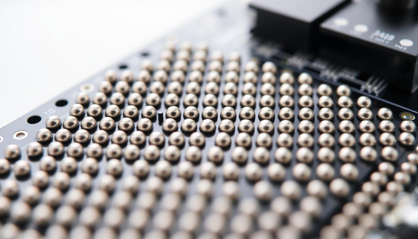
Ball Grid Array is a surface-mount packaging technology that uses an array of solder balls arranged in a grid pattern on the underside of the component. Unlike traditional leaded packages with pins around the perimeter, BGAs distribute connections across the entire bottom surface, creating a more compact footprint while supporting higher pin counts.
The solder balls serve as both electrical and mechanical connections between the integrated circuit and the printed circuit board (PCB). When heated during the reflow soldering process, these balls melt and form reliable interconnections with corresponding pads on the PCB.
Types of BGA Packages
| BGA Type | Substrate Material | Pitch Range | Thermal Performance | Applications |
| PBGA (Plastic BGA) | Plastic/Organic | 0.8-1.0mm | 15-20°C/W | Consumer electronics, memory modules |
| CBGA (Ceramic BGA) | Ceramic | 1.0-1.27mm | 8-12°C/W | Military, aerospace, high-reliability systems |
| TBGA (Tape BGA) | Polyimide tape | 0.5-0.8mm | 18-25°C/W | Ultra-thin devices, smartphones |
| FCBGA (Flip-Chip BGA) | Organic/Laminate | 0.4-1.0mm | 5-10°C/W | High-performance processors, FPGAs |
| µBGA (Micro BGA) | Flex tape | 0.3-0.4mm | 22-30°C/W | Wearables, miniature devices |
Advantages of BGA Assembly
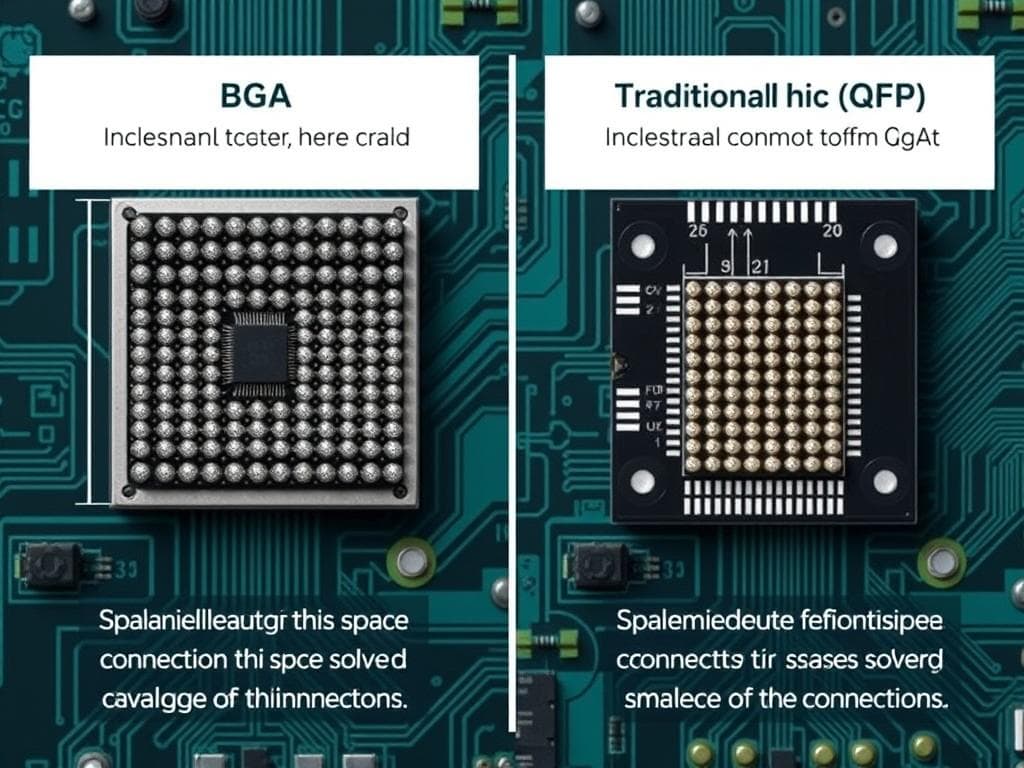
Advantages of BGA Technology
- Higher connection density (up to 1000+ I/O pins)
- Smaller footprint compared to leaded packages
- Improved electrical performance with shorter interconnects
- Better thermal dissipation through multiple solder balls
- Self-aligning during reflow due to surface tension
- Reduced inductance and capacitance for high-frequency applications
- Greater mechanical stability against vibration and shock
Limitations to Consider
- Hidden solder joints make visual inspection difficult
- Requires specialized X-ray equipment for quality control
- More complex PCB design with tighter tolerances
- Challenging rework process compared to leaded components
- Thermal expansion mismatch can cause reliability issues
- Higher manufacturing costs for low-volume production
The BGA Assembly Process Step-by-Step
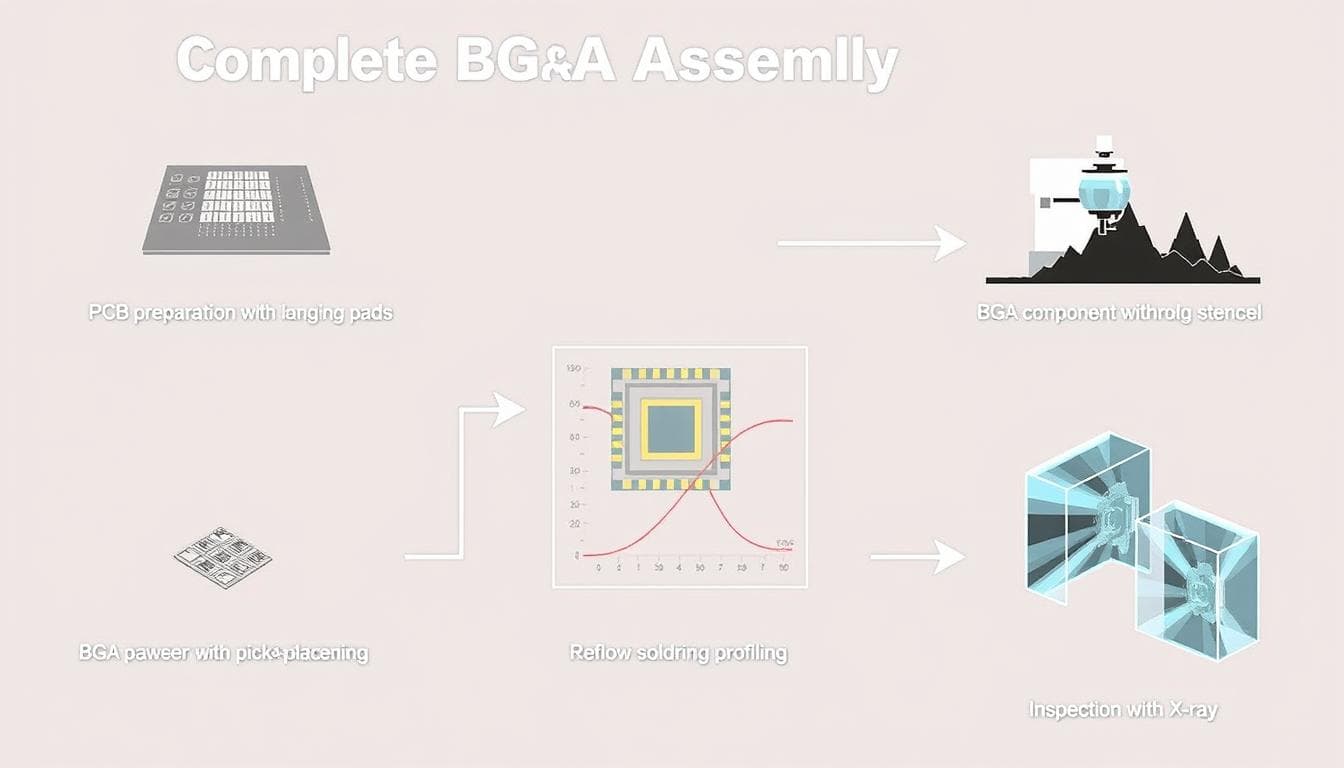
Successful BGA assembly requires precision at every stage of the process. The following steps outline the standard procedure for integrating BGA components onto a PCB:
- PCB Design and Preparation: Create appropriate landing pad patterns, typically using non-solder mask defined (NSMD) pads for pitches ≥0.5mm. For finer pitches, via-in-pad technology may be necessary.
- Solder Paste Application: Apply solder paste to the PCB pads using a precision stencil. For BGA components, circular apertures (100-150μm diameter) ensure uniform paste deposition.
- Component Placement: Position the BGA package precisely on the PCB using automated pick-and-place equipment. Alignment accuracy within ±0.05mm is crucial, especially for fine-pitch BGAs.
- Reflow Soldering: Pass the assembled PCB through a reflow oven following a carefully controlled temperature profile. For lead-free solder, peak temperatures typically range from 235-250°C with 45-90 seconds above liquidus (217°C).
- Cooling: Allow controlled cooling to prevent thermal shock and ensure proper solder joint formation. The cooling rate should be managed to minimize stress on the components.
- Inspection: Perform X-ray inspection to verify solder joint quality, checking for voids, bridges, or insufficient connections that aren't visible to the naked eye.
- Testing: Conduct electrical testing to confirm proper functionality, often using boundary scan (JTAG) techniques for high pin-count BGAs.
Critical Parameters for BGA Reflow Soldering
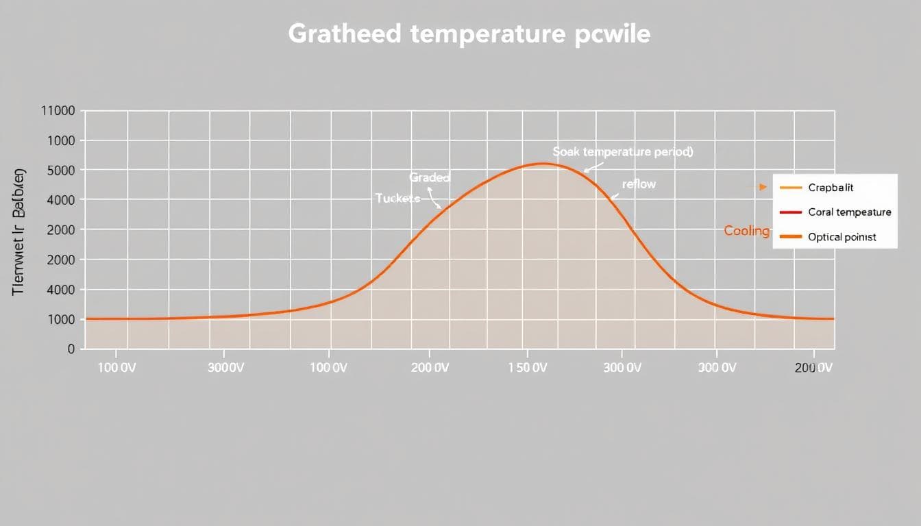
The reflow soldering process is particularly critical for BGA assembly. A properly controlled temperature profile ensures complete melting of solder balls while preventing component damage or solder defects.
| Reflow Phase | Temperature Range | Duration | Purpose |
| Preheat | 150-180°C | 60-90 seconds | Gradually warm components to prevent thermal shock |
| Soak | 180-200°C | 60-120 seconds | Activate flux and allow thermal equilibrium |
| Reflow | 235-250°C | 45-90 seconds | Melt solder and form interconnections |
| Cooling | 250°C to ambient | 1-3°C/second | Control solidification to prevent defects |
PCB Design Considerations for BGA Assembly
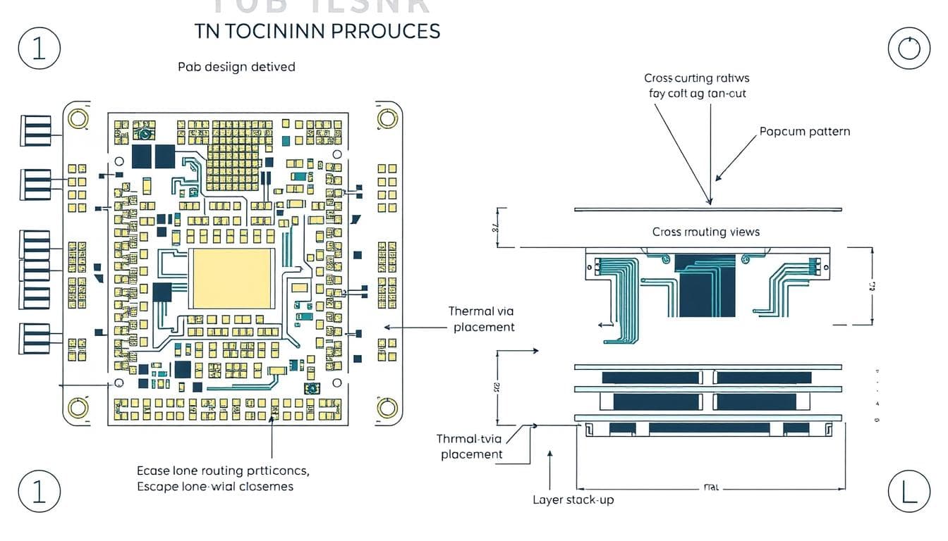
Successful BGA assembly begins with proper PCB design. The following considerations are essential for creating boards that support reliable BGA integration:
Pad Design and Layout
- Pad Type: Use non-solder mask defined (NSMD) pads for pitches ≥0.5mm. For finer pitches, consider solder mask defined (SMD) pads.
- Pad Size: Typically 80-85% of the solder ball diameter. For a 0.76mm ball, a pad diameter of 0.6-0.65mm is appropriate.
- Pad Finish: ENIG (Electroless Nickel Immersion Gold) or OSP (Organic Solderability Preservative) finishes provide excellent solderability for BGA applications.
- Solder Mask: Ensure precise solder mask registration with openings 0.05-0.1mm larger than the copper pad for NSMD designs.
- Fiducial Marks: Place at least two fiducial marks at opposite corners of the BGA footprint to aid in automated placement.
- Thermal Relief: Use thermal relief connections for pads connected to ground or power planes to ensure proper heating during reflow.
Routing Strategies
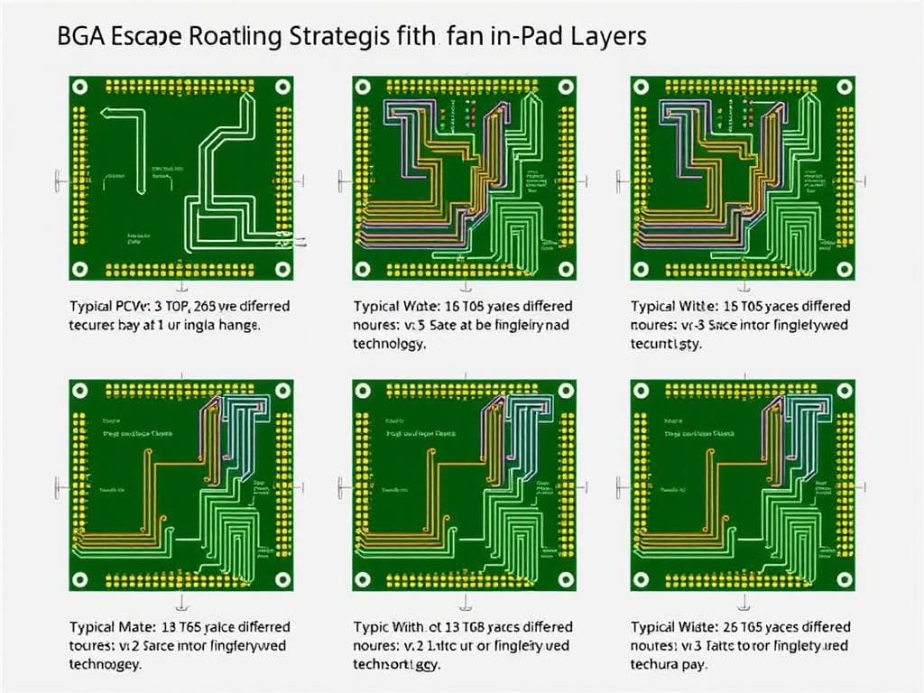
Routing connections from BGA pads to the rest of the circuit is one of the most challenging aspects of PCB design. Different strategies can be employed based on the BGA pitch and layer count:
Dog Bone Routing
- Suitable for BGAs with pitch ≥0.65mm
- Uses short traces to connect pads to nearby vias
- Requires less sophisticated PCB technology
- Typically needs 4-6 layer boards for moderate pin counts
Via-in-Pad Technology
- Essential for fine-pitch BGAs (≤0.5mm)
- Places vias directly in the BGA pads
- Requires filled and plated-over vias to prevent solder wicking
- Enables higher routing density but increases manufacturing cost
Common Challenges in BGA Assembly
Despite its advantages, BGA assembly presents several challenges that must be addressed to ensure reliable performance. Understanding these issues and their causes is essential for implementing effective solutions.
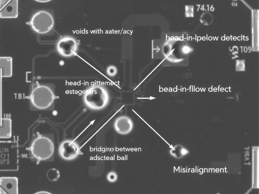
Solder Joint Voids
Voids are gas pockets trapped within solder joints during reflow. When voids exceed 25% of the joint volume, they can compromise electrical and thermal performance.
Causes: Outgassing from flux, moisture in components, improper reflow profile
Solutions: Vacuum reflow, nitrogen atmosphere, optimized temperature profile, quality solder paste
Head-in-Pillow Defects
A condition where the solder ball and paste make contact but don't fully coalesce, creating a weak joint that may pass initial testing but fail later.
Causes: Oxidized solder balls, warped components, insufficient heat
Solutions: Proper component storage, optimized reflow profile, enhanced flux activity
Solder Bridging
Occurs when solder forms unwanted connections between adjacent balls, creating short circuits that can cause device failure.
Causes: Excessive solder paste, component misalignment, improper stencil design
Solutions: Precise stencil design, controlled paste volume, accurate component placement
Request Your PCB/PCBA Quote
Looking for an accurate and fast PCB or PCBA quotation? Our engineering team is ready to review your files, provide pricing options, and offer the best manufacturing solution for your project.
Contact Us for a QuoteThermal Management Challenges
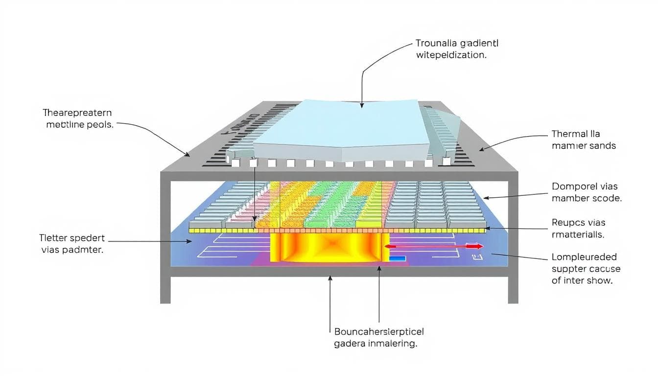
High-performance BGAs can generate significant heat during operation. Effective thermal management is crucial to prevent overheating and ensure long-term reliability.
Thermal Via Implementation
- Place thermal vias (0.2-0.3mm diameter) under the BGA to conduct heat to inner or bottom copper layers
- Typical density: 4-6 vias/cm² for effective heat dissipation
- Consider filled vias to prevent solder wicking during assembly
- Connect vias to internal copper planes for improved heat spreading
Material Selection
- Choose PCB substrates with thermal conductivity appropriate for the application
- Consider high-Tg (glass transition temperature) materials for high-temperature applications
- Match coefficient of thermal expansion (CTE) between PCB and BGA package
- Use thermal interface materials when attaching heat sinks to BGA packages
Inspection and Testing Techniques
Due to the hidden nature of BGA solder joints, specialized inspection and testing methods are essential to verify assembly quality and ensure reliability.
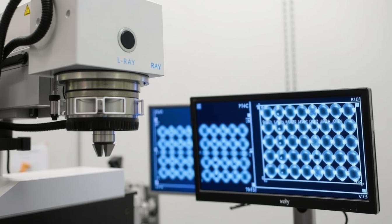
X-ray Inspection
X-ray inspection is the primary method for examining BGA solder joints. Modern systems provide detailed images that reveal internal defects invisible to optical inspection.
2D X-ray Inspection
- Provides top-down view of solder joints
- Detects bridging, missing balls, and gross voiding
- Limited ability to distinguish overlapping features
- More affordable and faster than 3D systems
3D/CT X-ray Inspection
- Creates three-dimensional images of solder joints
- Precisely measures void percentage and location
- Detects subtle defects like head-in-pillow
- Higher cost but provides more detailed analysis
Additional Testing Methods
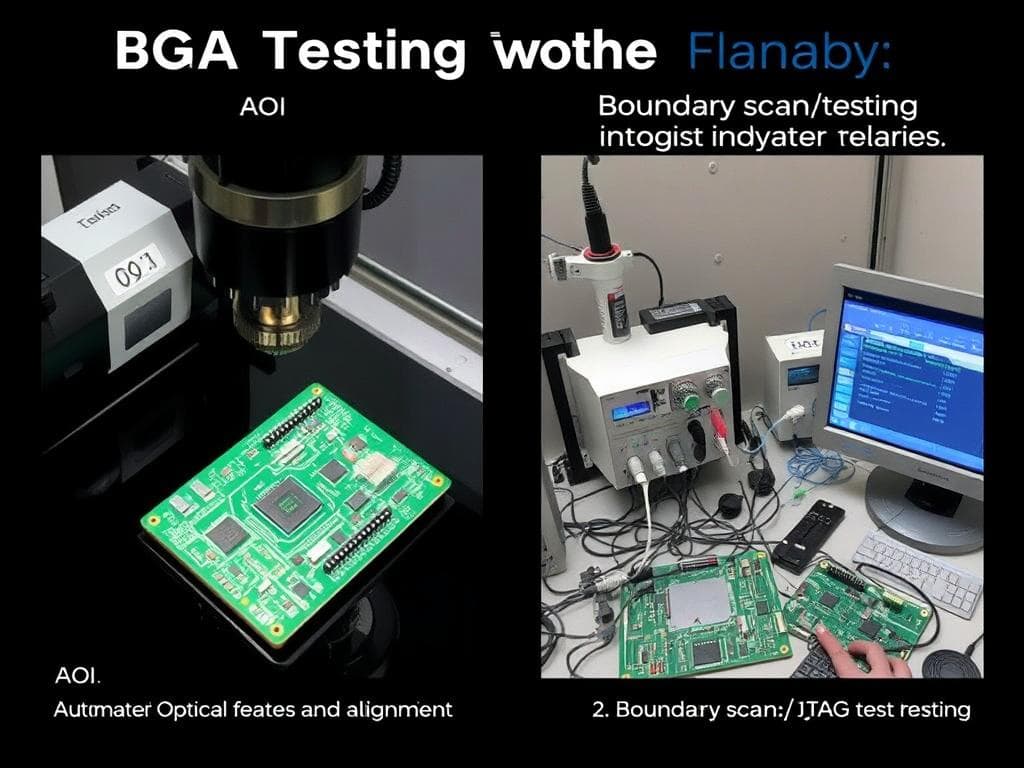
Automated Optical Inspection (AOI)
While AOI cannot see under BGA packages, it remains valuable for verifying component placement, orientation, and peripheral solder joints.
Modern AOI systems use multiple angled cameras to inspect the visible edges of BGA packages for proper alignment and seating.
Boundary Scan Testing
Also known as JTAG testing (IEEE 1149.1), this method uses built-in test circuits within the BGA to verify electrical connections without physical probing.
Particularly valuable for high-pin-count BGAs where traditional in-circuit testing is impractical.
Thermal Imaging
Infrared cameras detect temperature variations across the BGA during operation, helping identify poor connections that cause localized heating.
Useful for both quality control and troubleshooting field failures in BGA-mounted components.
Applications Across Industries
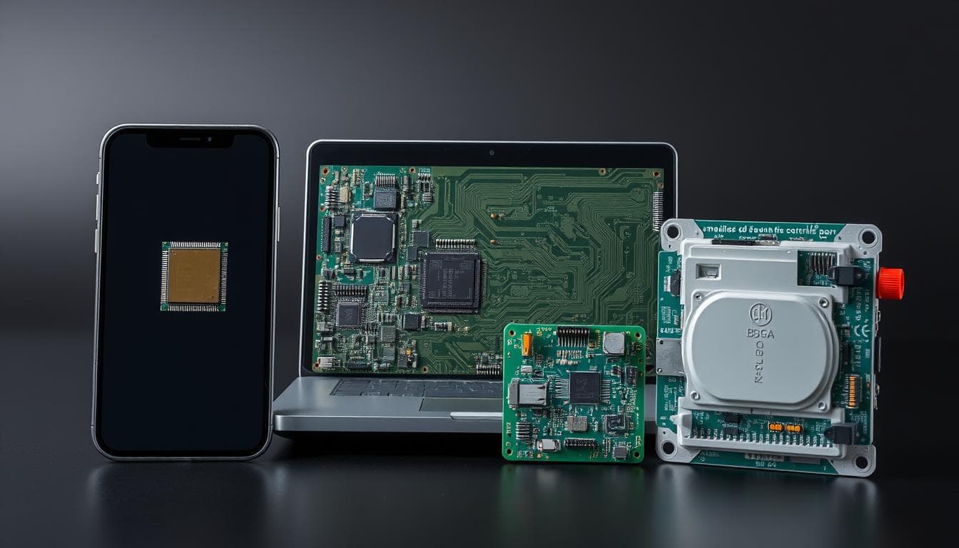
BGA technology has become ubiquitous across numerous industries, enabling the development of increasingly powerful and compact electronic devices.
Consumer Electronics
- Smartphones and tablets (application processors, memory)
- Laptops and desktop computers (CPUs, GPUs, chipsets)
- Gaming consoles (main processors, memory controllers)
- Digital cameras (image processors, memory)
Industrial and Automotive
- Engine control units and vehicle safety systems
- Industrial automation controllers and PLCs
- Power management systems
- High-reliability computing systems
Telecommunications and Networking
- Network switches and routers (network processors)
- Base station equipment (signal processors)
- Satellite communication systems
- High-speed data processing equipment
Medical Devices
- Patient monitoring equipment
- Diagnostic imaging systems
- Implantable medical devices
- Portable medical testing equipment
Aerospace and Defense
- Avionics systems
- Satellite communications
- Radar and signal processing equipment
- Mission-critical control systems
Future Trends in BGA Technology
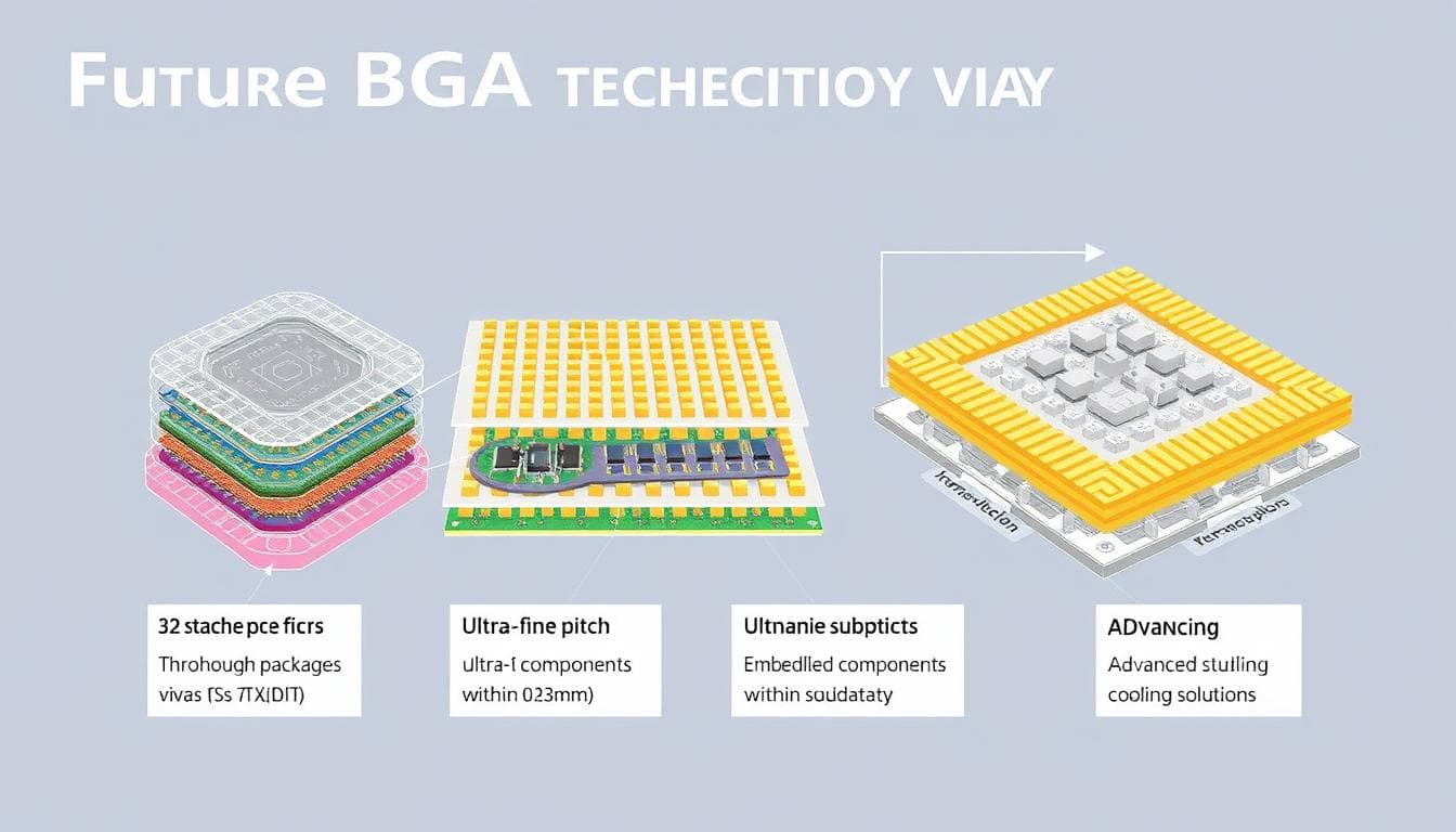
As electronics continue to evolve, BGA technology is advancing to meet new challenges in miniaturization, performance, and reliability.
Finer Pitch and Higher Density
The trend toward smaller ball pitch (below 0.3mm) continues, enabling more connections in the same footprint. This drives innovations in PCB manufacturing and assembly processes to maintain reliability at these reduced dimensions.
3D Packaging and Stacking
Vertical integration of multiple dies within a single BGA package using through-silicon vias (TSVs) and interposers is becoming more common, enabling higher performance and smaller form factors.
Enhanced Thermal Solutions
As power densities increase, advanced thermal management techniques like integrated microfluidic cooling channels and phase-change materials are being developed to maintain acceptable operating temperatures.
Conclusion
BGA assembly has transformed electronic manufacturing by enabling higher component density, improved performance, and enhanced reliability in a compact footprint. While the technology presents challenges in design, assembly, and inspection, these can be overcome through proper planning, process control, and specialized testing methods.
As electronic devices continue to shrink while demanding greater functionality, mastering BGA assembly techniques becomes increasingly important for manufacturers and engineers. By understanding the fundamentals outlined in this guide and staying current with evolving best practices, you can successfully implement BGA technology in your electronic designs.
Need Expert Assistance with Your BGA Assembly?
Our team of specialists can help you navigate the complexities of BGA design, assembly, and testing. From prototype to production, we provide comprehensive solutions tailored to your specific requirements.
Request Consultation