
What is PCB prototyping?
PCB prototyping means making printed circuit boards before mass production. Engineers design the circuit. Then they ask a board factory to make a small number of boards first. This step is for testing. Only when the prototype meets the test standards should the customer start full production. Prototyping lowers the risk of big mistakes in mass production. A printed circuit board is a very important part of any electronic product. Here are the usual steps of PCB prototyping.
Inner Layer Pattern (Inner Circuit)
First, the copper clad laminate is cut to the right size for the process. Before the dry film photoresist is applied, the copper surface is made slightly rough to help glue stick. Then a dry film photoresist is pressed on the copper at the right temperature and pressure. Next the board goes into a UV exposure machine. The circuit image on the film is transferred to the dry film photoresist on the board. After the top protective film is peeled off, the unexposed parts of the resist are removed with a sodium carbonate (alkaline) solution. After that, a hydrogen peroxide-based solution is used to etch away the exposed copper, so the circuit pattern forms. Finally, the remaining dry film photoresist is washed off with a mild alkaline solution (for example, dilute sodium hydroxide) or another approved stripper.
Lamination (Pressing Layers Together)
Before lamination, inner layers get a black oxide or other oxidation treatment. This makes the copper surface rough and helps glue stick. For multilayer boards (for example, six layers and above), the inner patterned layers are aligned with tooling pins or by a rivet/stacking method. The layers are stacked with prepreg sheets and put between polished steel plates. Then the stack is put into a vacuum press. The press uses the right temperature and pressure to harden the prepreg and bond all layers into one board. After lamination, machines with X-ray or optical alignment drill reference holes. The board edges are cut to the right size for later steps.
Pad and Contact Treatment
Solder mask covers most copper areas. The board leaves exposed pads for components, test points, and connector contacts. These exposed pads need a protective finish to avoid oxidation. The finish must protect the board during storage and use so reliability is good.
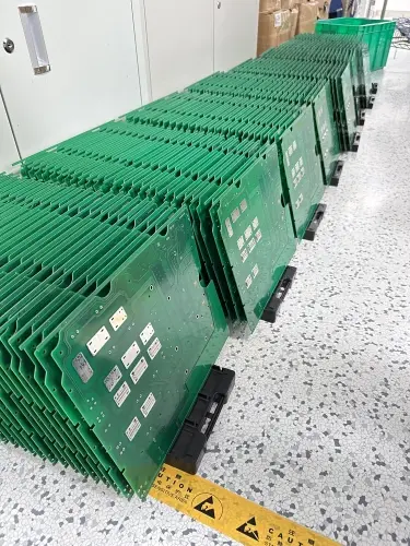
Routing and Final Cut (Board Shape)
The board is cut to the final shape by a CNC routing machine. After routing, dust and ionic dirt on the board are washed off.
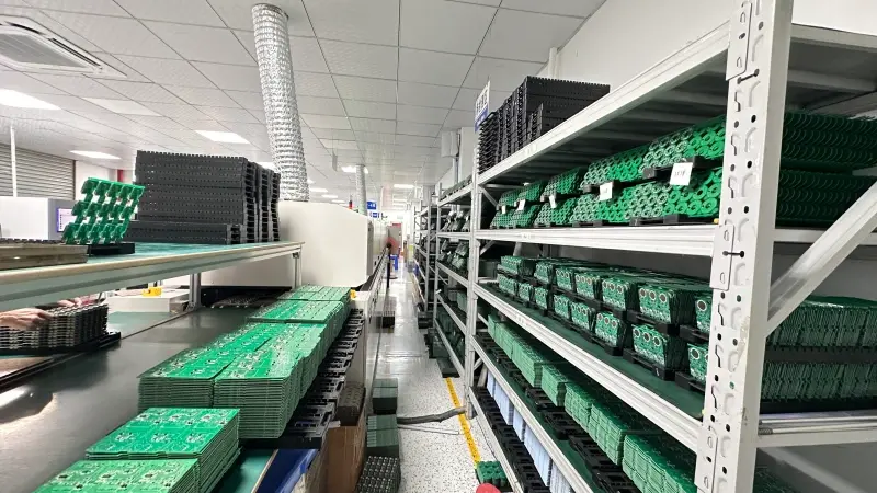
Inspection and Packing
At the end, the boards are inspected and then packed. Common packing ways include PE bag, heat-shrink wrap, and vacuum pack.
Differences Between PCB Manufacturing and PCB Prototyping (Clear Comparison)
The text you gave had extra content that mixed other topics. Here I give a clear and simple comparison between PCB mass production and PCB prototyping:
- Purpose
- Prototyping is for testing one design before mass production.
- Mass production is for making many boards after the design is proven.
- Purpose
- Quantity
- Prototypes are small number runs.
- Mass production is large number runs.
- Quantity
- Time
- Prototypes are made fast so engineers can test quickly.
- Mass production takes more time to set up, but then makes many boards faster per unit.
- Time
- Cost
- Per unit cost of prototypes is higher.
- Per unit cost in mass production is lower because of scale.
- Cost
- Quality and Control
- Prototypes focus on checking function, fit, and some process checks.
- Mass production uses more complete quality systems and tests to keep every board within spec.
- Quality and Control
- Process Flexibility
- Prototyping can use more manual checks and special runs.
- Mass production needs stable, repeatable steps and tight control.
- Process Flexibility
Philifast’s Problem-Solving Story: How We Help Customers with PCB Prototyping
Philifast is our company. We make PCBs and do prototyping work. We often meet customers who bring us designs that have problems. We help them find and fix these problems before full production. Here are common problems and how Philifast solves them. I keep the story clear and simple.
Problem 1: Wrong package or footprint
A customer gives us a design. We check the footprints. Then we find some packages do not fit the board pads. This makes soldering hard or makes parts fall off. We tell the customer the exact pin map and pad size. We show simple drawings and the expected pad sizes. Then the customer fixes the footprint. We make a new prototype and test it. The part fits and soldering works.
Problem 2: Signal or power noise
A design has high-speed signals. We check the board layout and the layer stack. We look at return paths and ground plane splits. We suggest simple fixes: move ground near the signal, add proper decoupling, or change trace width. We explain why the change helps in plain words. We build the prototype with the change. Then tests show less noise and the board works more stable.
Problem 3: Wrong hole size or drill tolerance
Sometimes holes are too small for the chosen pins. We check the drill chart and the component maker’s mechanical drawing. We pick the right drill size with enough tolerance. We make a test board. The pins go in easily. The assembly time drops.
Problem 4: Surface finish or solder mask conflicts
A contact or pad may need a special finish like ENIG or HASL lead-free. We test the finish on sample boards. We confirm the finish works with the assembly process. We also test the solder mask clearance near pads that need to be exposed. The result is reliable soldering.
Problem 5: Thermal or mechanical issues
If a design has heavy components, solder joints can break from heat cycles. We suggest strengthening pads, adding thermal relief, or using thicker copper. We test a prototype with thermal and mechanical checks. The board survives the test.
How Philifast works in these cases (simple steps):
- Customer sends design files and BOM.
- We run a design-for-manufacturing (DFM) check.
- We report the issues in plain words and suggest changes.
- Customer approves changes or asks questions.
- We make the prototype with agreed specs.
- We test or help the customer test.
- If tests pass, we move to mass production. If not, we repeat steps 2–6.
This way we solve real problems before full production. The customer saves time and money.
PCB Prototyping — Key Things to Watch (Story Form, Simple Rules)
When we do prototyping at Philifast, we watch some key things. We treat these as simple rules. We tell the customer each rule in plain words. Here are the rules:
- Choose the right prototype quantity
Order enough boards to test function, assembly, and a small reliability run. But do not order too many. This keeps cost low.
- Choose the right prototype quantity
- Confirm component packages
Check every package and footprint. A wrong footprint can fail the whole test. We use the BOM and the part drawings to confirm.
- Confirm component packages
- Do full electrical checks
We do a full netlist check and confirm layers, vias, and connectivity. This reduces rework later.
- Do full electrical checks
- Mind signal integrity and layout
For high-speed lines use correct trace width and spacing. Keep return paths clear. Use ground plane as much as possible.
- Mind signal integrity and layout
- Document tests and results
We write simple test steps and the results. This helps repeat the test after changes.
- Document tests and results
- Plan for assembly
Make sure fiducials, test points, and part orientation are clear. This helps automated assembly and reduces mistakes.
- Plan for assembly
Prototype Parameters Table (Philifast Typical Prototype Specs)
| Parameter | Typical Prototype Spec | Notes |
|---|---|---|
| Board material | FR-4 (standard) | Other materials on request |
| Max layers | 2 to 8 (prototype) | Up to higher layers with lead time |
| Min trace width / spacing | 4 mil / 4 mil (0.1 mm) | 3/3 mil possible with design review |
| Minimum line/space for standard | 6 mil / 6 mil | Safer for quick protos |
| Min drill hole | 0.2 mm (8 mil) | 0.3 mm common for through holes |
| Typical board thickness | 1.6 mm | 0.8 mm, 1.0 mm, 2.0 mm also common |
| Copper weight (inner/outer) | 1 oz (35 μm) | 0.5 oz or 2 oz on request |
| Surface finish | ENIG or Lead-free HASL (OSP on request) | ENIG is common for fine pitch |
| Soldermask color | Green standard | Other colors available |
| Silkscreen | White (top) | Black or other colors available |
| Impedance control | ±10% | Provide stackup and target impedance |
| Minimum annular ring | 4 mil (0.1 mm) | Depends on hole size |
| PCB panelization | V-score or routing | We can panelize for assembly |
| Electrical test | E-test (100%) | Option: flying probe |
| Surface cleanliness | IPC class per request | Standard cleaning done |
| Tolerance | ±0.1 mm on outline | Depends on thickness and process |
| Typical lead time | 3–7 working days | Depends on qty and finish |
| Packing | Vacuum or PE bag | Foam between boards for heavy parts |
| Special processes | Controlled depth routing, microvias | Ask for quotes |
Note: These values are typical. Tell Philifast your exact needs and we will confirm.
Final Notes and Simple Checklist (For Engineers)
Before sending your PCB for prototyping, check this list:
- Files: Send Gerber, drill file, and BOM.
- Footprints: Confirm each package and pad.
- Stackup: Give the layer stack and copper weight.
- Impedance: Provide target impedance and test points.
- Holes: Confirm via size and mechanical holes.
- Surface finish: Choose ENIG/HASL/OSP.
- Solder mask: Check mask clearance on pads.
- Test: Plan electrical test and assembly test.
- Quantity: Order just enough to test function and assembly.
- Communication: Tell Philifast any special needs in plain words.
