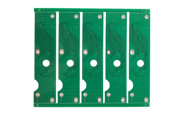
PCB is often called the “mother of electronics.” Computers, phones, and today’s electric vehicles all need PCBs. A PCB is a multi-layer platform that holds and links electronic parts to form circuits. It is like the skeleton of an electronic device. Parts are mounted on it. After parts are mounted, the board becomes a PCBA (PCB Assembly).
What’s a PCB Made Of?
A PCB is made from non-conductive material with copper layers. The copper layers form complex conductive paths and pads. Makers create these paths by etching the copper.
Basic PCB Structure
A typical PCB is a sandwich. A two-layer board has a copper layer on top and a copper layer on the bottom. Between them is a layer of fr4. fr4 is an epoxy glass fiber. It is not conductive. It separates the two copper layers.
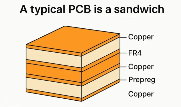
If we need a four-layer board, we press two two-layer boards together. We add a sheet called a prepreg between them. Prepreg is also an insulator. In simple terms, a six-layer board is three two-layer boards pressed together. An eight-layer board is four two-layer boards. So board layers increase in multiples of two.
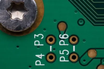
Solder Mask
On top of the copper, manufacturers apply a coat of paint called the solder mask. The solder mask protects the copper traces from air and oxidation. If the solder mask fails, the copper and pads can oxidize. That makes soldering hard or impossible.
The solder mask also keeps solder only on pads. The mask leaves the pads exposed. All other areas are covered so solder will not stick. That is why it is called a solder mask. It protects the circuit and isolates the pads.
Silkscreen
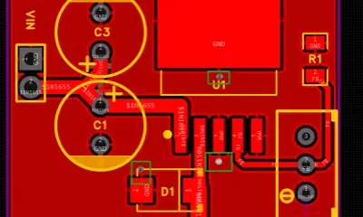
Above the solder mask, makers print a layer called the silkscreen. Silkscreen prints text and reference designators. During PCB assembly, these marks help people find parts. For example:
- C33 means capacitor number 33.
- R48 means resistor number 48.
| Reference Designator | Component Type | Description |
|---|---|---|
| R | Resistor | Passive component that resists the flow of electric current |
| C | Capacitor | Passive component that stores electrical energy |
| L | Inductor | Passive component that stores energy in a magnetic field |
| D | Diode | Semiconductor that allows current flow in one direction |
| Q | Transistor | Semiconductor used to amplify or switch electronic signals |
| U | Integrated Circuit (IC) | Complex circuit with multiple components on a single chip |
| LED | Light Emitting Diode | Semiconductor that emits light when current passes through |
| J | Connector/Jumper | Component used to connect different parts of a circuit |
| F | Fuse | Safety device that protects circuits from overcurrent |
| SW | Switch | Component used to open or close an electrical circuit |
The silkscreen uses short labels and simple marks. It helps assembly and repair.
Basic PCB Production Flow
Below are the main steps in PCB production. I use simple words and direct steps so this is easy to read.
Gerber Files
How do engineers draw PCBs? They make layer images. One common output is the Gerber file. Gerber files are the image files for each layer. They are like photo negatives. Black areas show places that are clear. Red areas show places that are opaque.
Engineers send Gerber files to the PCB maker. The maker uses the files to make films. These films guide the whole board production. A Gerber file is also called a photoplot or phototool.
Cutting the Raw Board (Cutting Panels)
Cutting the raw board means cutting the copper-clad laminate into production panels. Producers usually cut squares that fit the production line.
Before we go into more steps, here are three common words used in production:
- UNIT: A unit is a single PCB design drawn by the engineer.
- SET: A set is many units placed together. Engineers do this to save time and make production easier. This is often called panelization. A set includes the unit images, tool edges, and other marks.
- PANEL: A panel is the actual board that the factory makes. A panel can include several sets plus tooling strips and extra edges for handling. Panels help increase production efficiency.
Inner layer dry film (inner layer imaging)
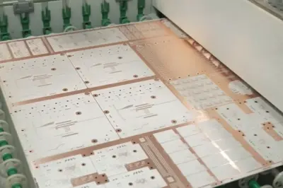
Inner layer dry film means transferring inner copper patterns to the inner copper foil. First, the maker adds a photo-sensitive film to the copper surface. This film hardens when light hits it. The board is then exposed through a film. The areas that get light harden. The dark areas stay soft.
Next, they develop the board. The soft film washes away. The hardened film remains and protects the copper. Then the board is etched. The etching removes unprotected copper. After stripping the film, the inner layer copper patterns remain on the board.
For designers, the main concerns are minimum trace width, spacing, and routing uniformity. If spacing is too small, the film cannot be fully removed. That causes shorts. If trace width is too thin, the film may not stick well and traces can open. So designers must plan safe spacing between traces, between a trace and a pad, and between pads.
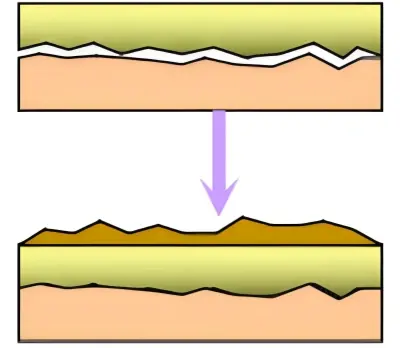
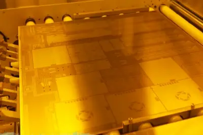
Brown oxide treatment (copper surface roughening)
Purpose: Make the inner copper surface slightly rough and add an organic metal layer. This helps glue the layers together.
How it works: Chemical treatment forms a uniform organic-metal layer on the copper. The layer bonds well to the prepreg. This improves adhesion between inner copper and prepreg when the board is pressed later.
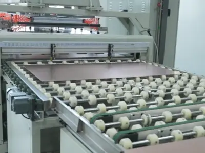
Lamination
Lamination bonds the copper layers and prepreg into one board. The process uses heat and pressure. The bond forms by diffusion and interweaving of polymers between layers. The factory stacks copper foils, prepreg, inner layers, steel plates, separation sheets, kraft paper, and outer steel plates per the process.
For designers, lamination symmetry matters. During lamination, heat and pressure create stresses inside the board. If the stack is not symmetric, these stresses differ on each side. That makes the finished board warp. Warping affects PCB performance.
Also, uneven copper distribution causes uneven resin flow. Areas with less copper become slightly thinner. Areas with more copper become slightly thicker. To avoid these problems, designers must consider copper balance, layer stack symmetry, and the placement of blind or buried vias.
Drilling
Drilling makes holes between layers. Drilling creates vias and through-holes that connect layers electrically.
Electroless copper (PTH – plated through hole)
After drilling, we need to make the hole walls conductive. The first step is electroless copper deposition. This step is also called chemical copper. The drilled board goes into a copper bath. A chemical redox reaction deposits a thin copper layer inside the holes. This makes the previously insulating substrate conductive and connects the layers.
After electroless copper, the board goes to electroplating. Electroplating thickens the copper on the surface and in the holes to about 5–8 µm. This prevents oxidation or micro-etching of the thin copper before further pattern plating.
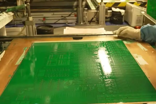
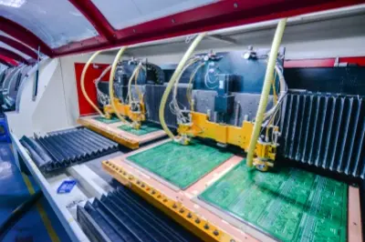
Solder mask (again)
Solder mask, also called green mask or UV mask, is one of the key steps. Factories apply solder mask by screen printing or coating. Then they expose and develop it. The process opens the pads and holes that must be soldered. All other areas get covered. This prevents short circuits during soldering.
Silkscreen printing
Silkscreen applies needed text, logos, and part marks. A screen prints the markings on the board. Then the board is exposed to UV light and cured.
Surface finish
Bare copper is solderable, but it oxidizes in air. Oxide makes soldering and long-term contact poor. So we apply a surface finish. The main purpose is to ensure good solderability and stable electrical properties.
Common surface finishes:
- HASL (Hot Air Solder Leveling) — also called spray tin in some texts. It coats the board in solder and levels it with hot air.
- ENIG (Electroless Nickel Immersion Gold) — also called immersion gold. It is nickel followed by a thin gold layer.
- OSP (Organic Solderability Preservative) — a water-based organic film that protects copper until assembly.
- Immersion tin — a thin tin layer.
- Immersion silver — a thin silver layer.
- Nickel-palladium-gold (ENEPIG) — nickel, then palladium, then gold.
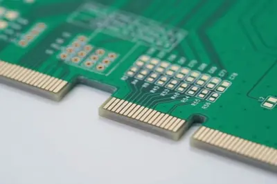
- Electroplated hard gold — thicker hard gold for edge connectors and fingers.
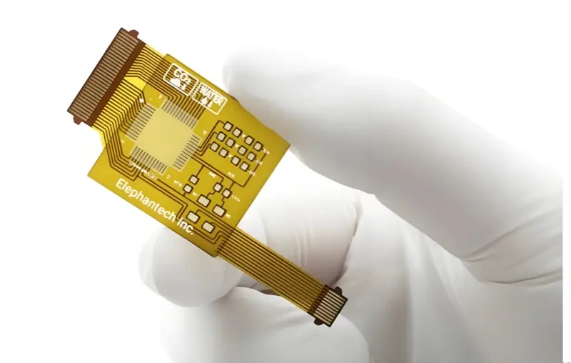
- Gold fingers — edge connectors plated with hard gold for wear resistance.
Each finish has trade-offs in cost, shelf life, solderability, and reliability. Choose the finish based on product needs.
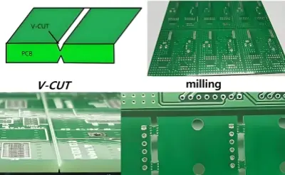
Routing / V-scoring / Shape forming
After surface finish, factories cut the boards to final outline with CNC routing or V-scoring. They make the board the shape the customer needs.
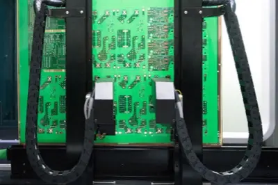
Electrical test (E-test)
Makers test the boards by simulating circuit conditions. They check for opens and shorts. This step finds defects before assembly.
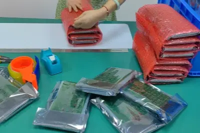
Final inspection, sampling, packaging
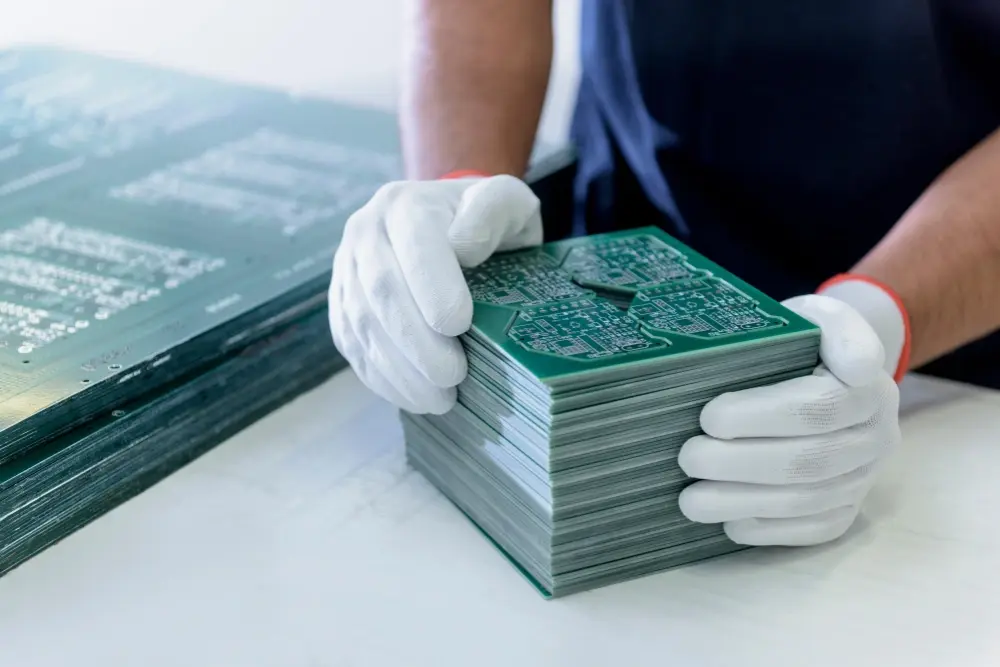
Factories inspect appearance, size, hole diameters, board thickness, markings, and other requirements. They ensure boards meet customer specs. Qualified boards go to packing. Factories pack the boards in bundles for storage and shipping.
Design Notes and Production Limits
Designers must think about manufacturing limits. Keep trace width and spacing within the plant’s capabilities. Avoid tiny annular rings around holes. Place copper evenly to reduce warping. Use symmetric stacks for multilayer boards. Consider blind and buried vias early because they affect layer count and lamination.
From PCB to PCBA
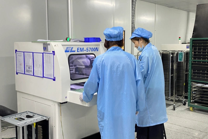
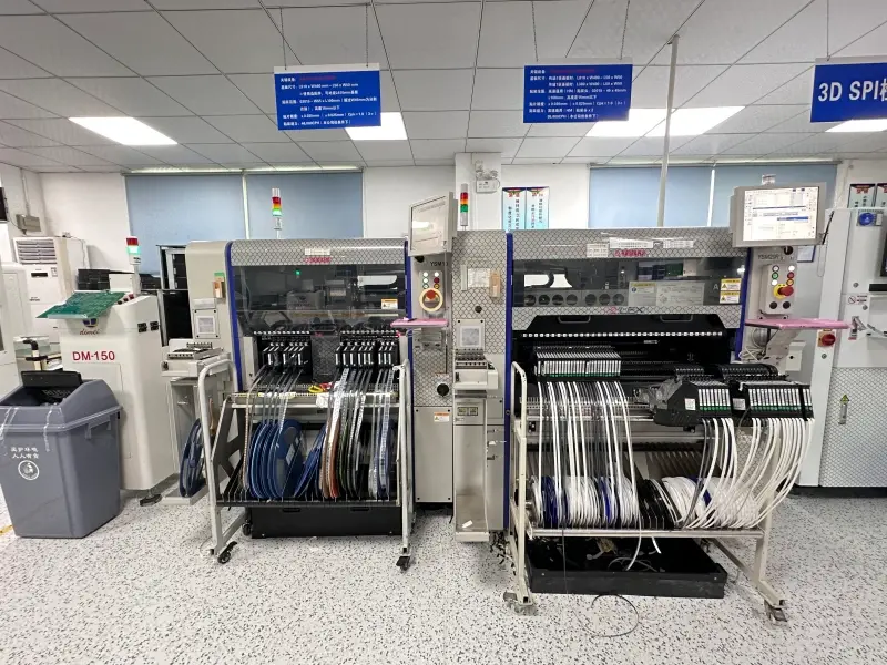
When parts are soldered onto the PCB, this becomes a PCBA. Assembly adds SMT and through-hole parts. The production process then includes pick-and-place, reflow soldering, wave soldering if needed, inspection, and functional test. A well-made PCB helps assembly go smoothly.
Summary
- PCB is a multi-layer board that holds and connects parts.
- fr4 is the common insulating material between copper layers.
- Solder mask protects copper and isolates pads.
- Silkscreen gives part labels for assembly.
- Gerber files drive production.
- Key steps: imaging, etching, brown oxide, lamination, drilling, electroless copper, electroplating, solder mask, silkscreen, surface finish, routing, testing, packing.
- Design must consider trace width, spacing, copper balance, and layer symmetry.
- After assembly, the PCB becomes a PCBA.