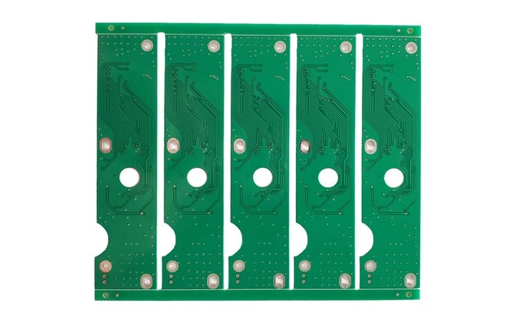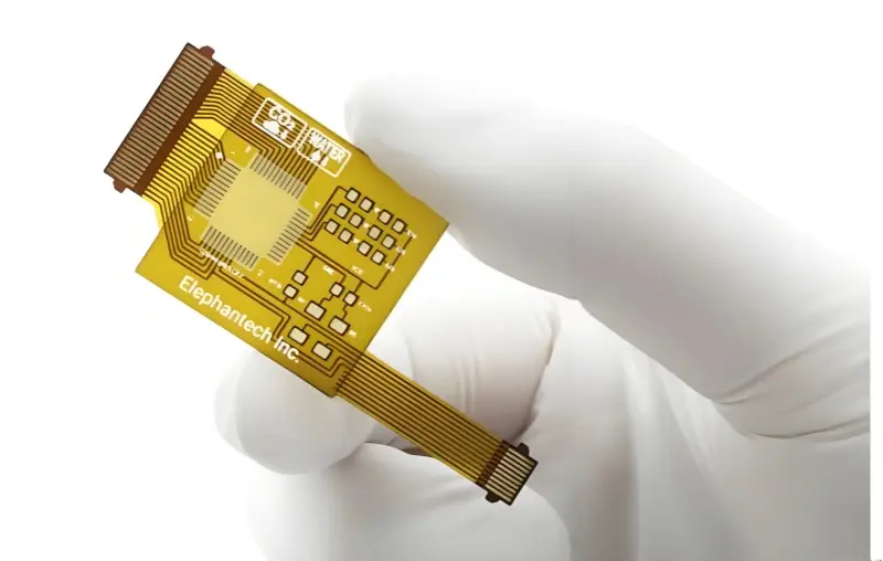
Introduction to SMT Stencils
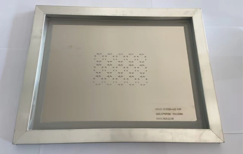
In the world of electronics manufacturing, there is a very important tool known as the “stencil.” You can think of a stencil as a very thin sheet made of steel. The size of this steel sheet is usually fixed and standard. This is because it needs to fit perfectly into a machine called a solder paste printer. Although the length and width are often standard, the thickness of the stencil can change. People choose different thicknesses based on what they need for a specific project. The thickness of these steel sheets can vary quite a bit. Common thicknesses include 0.08 millimeters, 0.10 millimeters, 0.12 millimeters, 0.15 millimeters, and 0.18 millimeters. Engineers will pick the right thickness depending on the specific components they are using.
The Purpose and Function of the Stencil
The main reason we use a stencil is for a process called “SMT,” which stands for Surface Mount Technology. In this process, we need to put solder paste onto the circuit board. Solder paste is a sticky, grey material that acts like glue and metal at the same time. The stencil is designed to make sure this solder paste goes exactly where it needs to go on the circuit board.
To do this, the stencil has many small holes cut into it. These holes are called “apertures.” When it is time to print the solder paste, the process follows a few simple steps. First, the worker or the machine puts the solder paste on the top side of the stencil. At the same time, the circuit board is placed directly under the stencil. The holes in the stencil line up perfectly with the metal pads on the circuit board.
Next, a tool called a “squeegee” is used. A squeegee is like a blade or a scraper. Because solder paste is thick and sticky, like toothpaste, the squeegee is used to push and wipe the paste across the top of the stencil. As the squeegee moves, it presses the solder paste down. The paste gets squeezed through the small holes in the stencil. It flows down and sticks to the circuit board underneath.
After the paste is applied, the stencil is lifted away. When you take the stencil away, you will see that the solder paste remains on the circuit board, but only in the exact shapes and places defined by the holes in the stencil.
To make this easier to understand, you can think of it like spray painting. Imagine you want to paint a specific shape on a wall. You would prepare a cover or a mask with that shape cut out of it. In this example, the stencil is the cover, and the solder paste is the paint. The cover has the pattern you want. When you spray paint over the cover, the paint only goes onto the wall where the holes are. The result is the exact shape you wanted. This is exactly how an SMT stencil works.
Types of SMT Stencils
We can classify SMT stencils into different groups based on how they are made. These types include:
Laser Stencils
Electropolished Stencils
Electroformed Stencils
Step Stencils
Bonding Stencils
Nickel-Plated Stencils
Etched Stencils
Let’s look at each of these types in more detail.
Laser Stencils
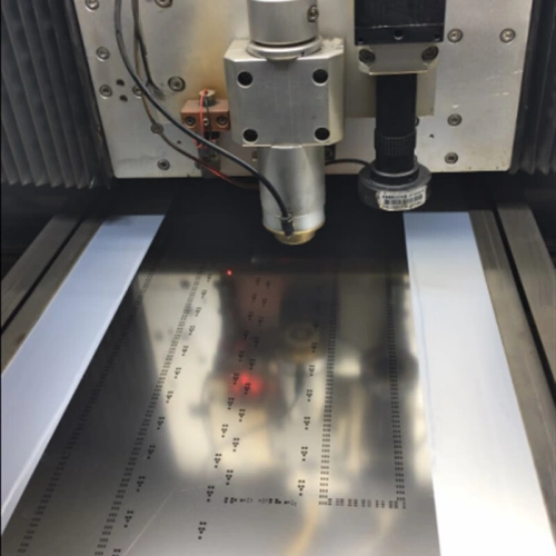
This is a very popular type of stencil. It is made using data files directly from the computer. Because it uses digital data, there are fewer steps in the making process. This reduces the chance of making mistakes. One of the biggest features of laser stencils is their high accuracy. The position of the openings is very precise. The error for the whole process is very small, usually less than or equal to plus or minus 4 micrometers. Also, the shape of the openings in a laser stencil is very good. The holes have a geometric shape that helps the solder paste form correctly when it is printed.
Electropolished Stencils (E.P. Stencils)
An electropolished stencil starts as a laser-cut stencil. After the laser cuts the holes, the steel sheet goes through a special process. This process uses chemicals and electricity to polish the steel. This is done to improve the walls of the holes. The main feature of this type is that the walls of the holes become very smooth. Because they are so smooth, the solder paste does not stick to the walls. This makes it perfect for very small and fine components, such as QFP, BGA, or CSP parts. Another benefit is that you do not need to clean or wipe the stencil as often. This saves time and makes the work more efficient.
Electroformed Stencils (E.F. Stencils)
Modern electronic products are changing. They are becoming shorter, smaller, lighter, and thinner. Because of this, the parts inside them are also getting smaller. We now see very tiny parts like the “0201” size and very tight spacing between parts, known as “ultra-fine pitch.” Examples of this are uBGA and CSP components. Because these parts are so small, the SMT industry needs better stencils. This is why the electroformed stencil was created. A key feature of this stencil is that you can have different thicknesses on the same sheet. This gives engineers more control.
Step Stencils
Sometimes, a single circuit board has many different types of parts on it. Some large parts need a lot of solder paste. Some small parts need very little solder paste. This means one thickness for the whole stencil might not work. To solve this, we use a “Step Stencil.” This stencil has different thicknesses in different areas. This creates a “Step-Down” or “Step-Up” effect. For a “Step-Down” stencil, the manufacturer makes specific areas of the stencil thinner. This reduces the amount of solder paste for the components in that area.
Bonding Stencils
Sometimes, a circuit board already has some parts attached to it before the solder paste printing step. For example, it might have “COB” (Chip On Board) devices already fixed in place. But, we still need to print solder paste for other parts. In this case, we use a Bonding Stencil. This stencil has a special design. It has a small “cap” or cover created at the spot where the COB device is on the board. This cap allows the stencil to fit over the existing part without hitting it. This keeps the stencil flat so it can print properly.
Nickel-Plated Stencils
This type of stencil combines the good points of laser stencils and electroformed stencils. The steel is plated with nickel. The purpose of this is to reduce friction. When the walls of the holes are slippery, the solder paste can slide out easily. This improves the release of the paste and makes the printing better.
Etched Stencils
These stencils are made using a specific type of steel, often imported 301 steel. Etched stencils are good for printing circuit boards where the spacing between parts is 0.4 millimeters or more. They are also suitable for copying boards or using film. You can use computer data (CAD/CAM) or exposure methods to make them. You can also change the size depending on the parts. You do not need to calculate the price based on how many parts there are. It is fast to make. Also, it is cheaper than laser stencils. It is convenient for customers who want to keep the film on file.
Classification by Manufacturing Method
Basically, we can divide SMT stencils into three main categories based on how they are built. These three methods are:
Chemical Etching Process
Laser Cutting Process
Electroforming Process
Let’s discuss how each one works, along with their good points and bad points.
Chemical Etching Method
This is the oldest method. First, a layer of protection that resists acid is put on a metal foil. Then, a tool with pins is used to align a film with the pattern on it. The pattern is exposed onto both sides of the metal foil. After that, the foil is put into chemicals that eat away the metal. This happens on both sides at the same time. The chemicals eat through the metal to form the openings.
Advantages: It forms the shape all at once. It is quite fast. It is also the cheapest option.
Disadvantages: It has a big problem with the shape of the hole. It tends to form a “hourglass” shape because the acid eats from both sides but not perfectly in the middle. This means the etching is not enough in the center. Or, sometimes the hole gets too big if it is etched too much. Also, human skill and the quality of the chemicals affect the result a lot. There are many steps, so errors can add up. It is not good for very fine or small parts. Finally, the chemicals used are dirty and bad for the environment.
Laser Cutting Method
This method uses the original data from the customer (called Gerber data) directly. It does not need film. A laser beam cuts the holes one by one. This method has very good accuracy and you can repeat it with the same results. Laser technology is also the only method that allows you to fix a stencil if there is a mistake.
Advantages: The data is very precise. Outside factors like human error do not affect it much. The shape of the hole is usually a trapezoid (wider at the bottom), which is good for releasing the paste. It can do very precise cutting. The price is moderate—not too cheap, not too expensive.
Disadvantages: The laser cuts the holes one by one. If there are many holes, it takes a longer time to make.
Electroforming Method
This is an “additive” process. This means it builds the stencil up, rather than cutting material away. It starts with a base board. A photo-sensitive material is put on it and developed to mark where the holes should be. Then, nickel atoms are added layer by layer around the photo material. This builds up the stencil.
Advantages: The walls of the holes are extremely smooth. This is the best method for ultra-fine spacing and very small parts.
Disadvantages: The process is hard to control. It uses chemicals that can pollute the environment. It takes a long time to make, and the price is very high.
New Technologies: 3D Stencils
As circuit boards become more complex and precise, the demand for reliability goes up. This has led to the invention of the “3D Stencil.” One example is the electroformed nickel “VectorGuard 3D stencil.” This is designed for printing on boards that are not flat. It can print on two different heights at the same time. In fact, it can handle height differences of up to 3 millimeters. Before this technology, if you had a tall part like a power transistor, you could not print paste near it easily. You would have to print the board first, and then dispense paste manually for the special parts. This was slow. The VectorGuard 3D stencil removes the need for this manual step. It makes the process simpler and improves productivity. However, traditional laser stencils are very mature and reliable today. Also, the VectorGuard 3D technology is expensive. Because of the high cost, it is still seen as a new field. People are studying it, but it is not yet used everywhere.
Cost Considerations
For many companies, cost is very important. Generally speaking, the price to open a mold for a normal stencil is between 300 and 600 Yuan. The exact price depends on the specifications. If you need a high-precision stencil, the price is around 1000 Yuan. If you are a startup company or in the research phase, you might only need to make a small number of prototype boards. In this case, controlling costs is very important. You need to balance quality with the price of the stencil.
SMT Stencils: Types & Manufacturing Methods Comparison Tables
Table 1: SMT Stencil Types Comparison
| Type | Key Features | Advantages | Disadvantages | Typical Applications |
|---|---|---|---|---|
| Laser Stencils | Digital data-driven production, high precision (±4μm error), trapezoidal hole shape | Fewer production steps, low error rate, precise hole positioning, good solder paste release | Longer production time for high-hole-count stencils | General SMT assembly, medium to fine-pitch components |
| Electropolished Stencils (E.P. Stencils) | Derived from laser-cut stencils, chemical + electrical polishing, smooth hole walls | No solder paste adhesion, less frequent cleaning, ideal for fine components | Higher cost than basic laser stencils | QFP, BGA, CSP components, fine-pitch applications |
| Electroformed Stencils (E.F. Stencils) | Additive manufacturing, variable thickness on single sheet | Suitable for ultra-fine pitch (0201 size, uBGA), excellent precision | Complex process control, high cost, environmental pollution risk | Miniaturized electronic products, ultra-fine pitch components |
| Step Stencils | Variable thickness in different areas (Step-Down/Step-Up) | Accommodates both large and small components on one PCB | More complex manufacturing, higher cost than standard stencils | PCBs with mixed component sizes (high solder paste demand variation) |
| Bonding Stencils | Special cap design for existing components | Fits over pre-mounted parts (e.g., COB), maintains flat printing surface | Custom design required, limited to specific PCB layouts | PCBs with pre-attached COB devices |
| Nickel-Plated Stencils | Nickel-plated steel, combines laser and electroformed stencil benefits | Reduced friction, improved solder paste release | Higher cost than basic laser stencils | Applications requiring enhanced paste release |
| Etched Stencils | Made from imported 301 steel, chemical etching or exposure process | Fast production, low cost, no part-count-based pricing | Hourglass-shaped holes, poor for fine-pitch components | PCBs with ≥0.4mm component spacing, prototypes, copy boards |
Table 2: SMT Stencil Manufacturing Methods Comparison
| Method | Process | Accuracy | Cost | Suitability | Environmental Impact |
|---|---|---|---|---|---|
| Chemical Etching | Acid-resistant coating → pattern exposure → double-sided chemical etching | Low (hourglass holes, human/chemical-dependent errors) | Lowest | Large-pitch components, cost-sensitive projects | High (hazardous chemicals) |
| Laser Cutting | Direct Gerber data input → laser beam cutting (hole-by-hole) | High (±4μm error, consistent repeatability) | Moderate | Most SMT applications, fine-pitch components, repairable stencils | Low (no harmful chemicals) |
| Electroforming | Photosensitive material coating → pattern development → nickel layer deposition | Highest (ultra-smooth hole walls) | Highest | Ultra-fine pitch components, miniaturized electronics | High (polluting chemicals) |
How to Determine the Size of a Stencil
When you order a stencil, you need to know the size. The size of a PCB stencil is made up of two parts: the “internal size” and the “overall size.” The internal size is the size that fits your specific circuit board. The overall size is the size of the whole frame that fits into the printing machine. You must design both sizes correctly so the stencil works well.
There is a simple rule to calculate the internal size:
For a stencil with a frame: The width = PCB width + 100mm. The length = PCB length + 100mm.
For a frameless stencil: The width = PCB width + 200mm. The length = PCB length + 200mm.
Let’s look at an example. Imagine you have a circuit board that is 50mm by 50mm. If you want a stencil with a frame, the size should be around 150mm by 150mm. If you want a frameless stencil, the size should be around 250mm by 250mm. This rule is easy to remember and easy to use. Because it is so simple, it was used a lot for manual printing before automatic machines became popular. We can say that the size of the PCB decides the internal size of the stencil.
However, when we talk about automatic solder paste printing machines, things are different. For these machines, the “overall size” is the most important thing. The overall size must be decided by the limits of the machine. The stencil must fit inside the machine’s frame.
If you are a PCB designer, you need to focus on the internal size. You usually do not need to worry about the overall size. The overall size is typically decided by the assembly factory you are working with, based on the machines they own.