
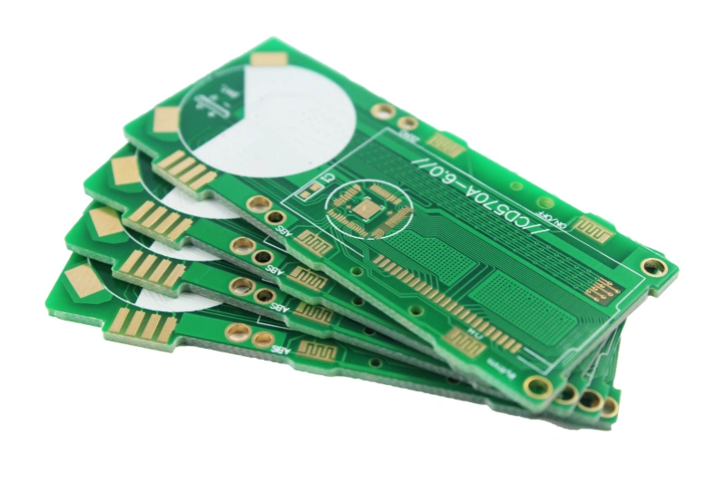
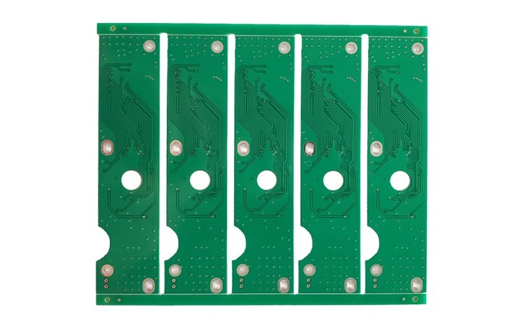
As high-speed circuits appear more and more, PCB complexity grows. To avoid electrical problems, signal layers and power layers must be separated. This leads to the need for multi-layer PCB design, that is, stackup design.
A good stackup design can improve power quality, lower crosstalk and EMI, and improve signal transmission. It can also save cost and make routing easier. Any high-speed PCB designer must think of stackup first.
01 Ten common rules for PCB stackup design
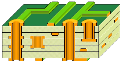
- Signal layers next to ground or power planes
In multi-layer PCBs, avoid having two signal layers next to each other. A typical board has signal layers (S), power planes (P), and ground planes (GND). Power and ground planes are usually solid and not split. They give the nearby signal traces a low-impedance return path. That is why signal layers are usually next to a power or ground plane. Power and ground use large copper pours. These copper pours also shield the signal traces. This helps control impedance and improve signal quality. Also, avoid putting two signal layers right next to each other. Adjacent signal layers cause crosstalk. This can make the circuit fail. Putting a ground plane between two signal layers stops most crosstalk. - Top and bottom are usually signal layers
The top and bottom layers of a multi-layer PCB often hold parts and some traces. So they are usually signal layers. Normally put parts on the top. The layer under the top can be a ground plane. That ground plane gives a reference for traces and shields parts. Also keep top and bottom traces short. Short traces reduce direct radiation. - Choose ground plane as reference first
Power and ground can both be reference planes and both can shield. The difference is that a power plane usually has higher characteristic impedance and a bigger potential difference from the reference. The ground plane is usually used as the ground reference. Ground gives a more stable reference and better shielding than the power plane. So choose ground as the reference plane first when you can. - Put high-speed signals in inner signal layers
High-speed signal layers should be inner signal layers. Put them between two copper planes. Then the two copper planes act as shields for the high-speed traces. This also keeps the radiation of those fast signals inside the two copper planes and reduces external interference. - Power and ground should appear in pairs
Power and ground should come in pairs. Make the distance between a power plane and its ground plane small. This lowers the power plane impedance. It helps power stability and lowers EMI. The main power plane should be next to its ground plane when possible. In high-speed designs, you can add extra ground planes to isolate signal layers. But do not add many power planes to isolate signal layers. Power planes can carry high-frequency noise. - Balance copper planes
Power or ground copper planes should be placed in a balanced way. For example, in a six-layer board, layer 2 and layer 5, or layer 3 and layer 4, should both be copper planes. This keeps the stackup balanced in the manufacturing process. Unbalanced copper layers can make the PCB warp when it heats or cools. - Keep multiple power planes away from high-speed signal layers
Multiple power planes should be far from high-speed digital traces. A power plane that is split into regions with different voltages can make a bad return path for signals. If a signal layer sits near a split power plane, the return current may not find a good path. This creates gaps in the return path and causes problems. - Use even number of layers
Classic PCB stackups use an even number of layers. Even-layer boards cost less and warp less than odd-layer boards. So choose an even layer count when you can. - Route pairs on nearby layers
Routing often needs layer changes. The two layers that a signal crosses form a routing pair. The best routing pair avoids making the return current go from one reference plane to another. The return current should stay inside one reference plane area. So put routing pairs on nearby layers. A path that crosses many layers makes the return current path poor. You can add decoupling capacitors near vias or reduce the dielectric thickness between reference planes to help. But it is better to plan routing so return current stays on one plane. - Make adjacent signal layers orthogonal in routing direction
On the same signal layer, keep most traces in one main direction. Make the routing direction on the adjacent signal layer cross it at right angles. For example, set one layer traces to run in the Y direction and the next layer to run in the X direction. This lowers crosstalk between layers.
These rules are a guide. In real designs, rules may conflict. You must weigh trade-offs and pick a good stackup.
Example choices for a four-layer board
Here are three example stackups for a common four-layer board. Choose based on your needs.
- Option A
Layer 1 (Top): S1
Layer 2: GND
Layer 3: P
Layer 4 (Bottom): S2 - Option B
Layer 1 (Top): S1
Layer 2: P
Layer 3: GND
Layer 4 (Bottom): S2 - Option C
Layer 1 (Top): P
Layer 2: S1
Layer 3: GND
Layer 4 (Bottom): S2
Option C is not good because power and ground do not couple well. Option A and B are both used. Designers often pick Option A for a four-layer board when parts sit on the top only. Option A gives a ground plane under the top parts and a power plane inside. If parts sit on both top and bottom and the dielectric between inner power and ground is thick, consider which side has fewer signal traces. For Option A, the bottom has fewer traces and can use a large copper pour to couple to the power plane. If parts are mostly on the bottom, pick Option B.
02 Common stackups for 4 to 10 layers
Here are common stackups for boards from 4 to 10 layers. Each stackup has pros and cons. Some are easier to route. Some have better EMC. Some give better signal integrity. Pick by what you need.
Four-layer board
- S1 – GND – P – S2
This is a common choice. Put the ground under the top layer. Put key signals on S1. Keep the distance between power and ground not too thick. Try to keep it under 5 mil. - S1 – P – GND – S2
If the bottom layer is the critical signal layer, use this. Place key signals on S2. - GND – S1 – S2 – P
This gives some shielding effect.
Six-layer board
- S1 – GND – S2 – S3 – P – S4
Use this when you need many routing layers and must control cost. In this layout S2 is the best routing layer. - S1 – S2 – GND – P – S3 – S4
Make the core between layer 3 and 4 thin to lower power impedance. Cross route layer 1 with 2, and cross route layer 5 with 6. The layer near the ground plane (S2) is a top routing layer. - S1 – GND1 – S2 – P – GND2 – S3
This is a popular layout. It has three routing layers, one power layer, and two ground layers. S2 is the best routing layer. Place high-speed signals on S2. Make the dielectric between layer 4 and 5 as thin as possible.
Eight-layer board
- S1 – GND1 – S2 – GND2 – P – S3 – GND3 – S4
This is a common choice. S2 is the best routing layer. - S1 – GND1 – S2 – P1 – GND2 – S3 – P2 – S4
Use this when you need many different power nets. Layer 3 and layer 6 are the best routing layers. - S1 – GND1 – S2 – S3 – P – S4 – GND2 – S5
This layout gives poor decoupling between power and ground. Use it when you need many routing layers and cost control, like in consumer tablets. S2 and S4 are good routing layers. Increase the distance between layer 3 and 4 and cross route layers.
Ten-layer board
- S1 – GND1 – S2 – S3 – GND2 – P – S4 – S5 – GND3 – S6
Use this when one power plane is enough. - S1 – GND1 – S2 – S3 – P1 – GND2 – S4 – S5 – P2 – S6
S2 and S4 are prime routing layers. - S1 – GND1 – S2 – GND2 – P1 – S3 – GND3 – S4 – P2 – GND4 – S5
Use this when EMC is strict and you need two power planes. S2 and S3 are prime routing layers. You can increase the distance between P1 and P2 when needed.
03 How to match stackup and impedance in manufacturing
After many design reviews, the PCB stackup is set. Now you must turn the design into a real board. This needs a proper lamination stack and good impedance control. Any board that needs impedance control must match the lamination and impedance before production. You must also calculate the required trace width and spacing.
One major way to meet impedance targets is to choose proper prepreg thickness. Philifast offers many common lamination choices for customers. These choices meet most needs on the market. The key of the lamination is the prepreg (PP) thickness. A thinner PP gives lower impedance. A thicker PP gives higher impedance. So change the PP thickness to match the needed impedance. When trace geometry is fixed, adjusting the PP thickness is the best choice.
Four-layer lamination example: Copper foil → Prepreg (PP) → Core → Prepreg (PP) → Copper foil
Philifast gives three common PP thickness options: 7628, 2116, and 1080. These cover most manufacturing needs.
Below are examples using a 1.6 mm, four-layer board. The data show how PP thickness affects calculated impedance.
7628 PP (PP thickness 0.200 mm)
- Layers: Copper foil, PP 7628 (0.2000 mm), Core (1.1000 mm), Core (1.1000 mm), PP 7628 (0.2000 mm), Copper foil.
- Typical finished copper thickness: 1 oz outer and inner.
- Example impedance results for L1 signal layer with L2 ground reference:
- 50 ohm single-ended: trace width ~13.00 mil → result ~50.35 ohm
- 90 ohm differential: trace width ~7.47 mil, spacing 4.00 mil → result ~90.00 ohm
- 100 ohm differential: trace width ~5.60 mil, spacing 4.00 mil → result ~100.69 ohm
2116 PP (PP thickness 0.125 mm)
- PP thickness 0.1250 mm. Core thickness 1.2000 mm.
- Example impedance results for L1 with L2 reference:
- 50 ohm single-ended: trace width ~7.42 mil → result ~50.00 ohm
- 90 ohm differential: trace width ~5.50 mil, spacing 4.00 mil → result ~90.90 ohm
- 100 ohm differential: trace width ~4.20 mil, spacing 4.00 mil → result ~100.31 ohm
1080 PP (PP thickness 0.080 mm)
- PP thickness 0.0800 mm. Core thickness 1.3000 mm.
- Example impedance results for L1 with L2 reference:
- 50 ohm single-ended: trace width ~4.12 mil → result ~50.70 ohm
- 90 ohm differential: trace width ~4.00 mil, spacing 4.80 mil → result ~90.62 ohm
- 100 ohm differential: trace width ~3.00 mil, spacing 4.50 mil → result ~100.74 ohm
Philifast can also auto-calculate the trace width and spacing needed for different stackups. This saves users from doing complex impedance math by hand. It makes impedance control easier and saves time.


