Introduction
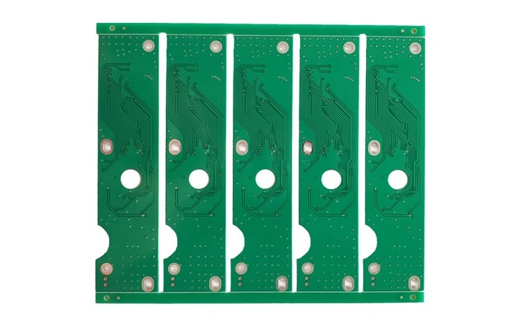
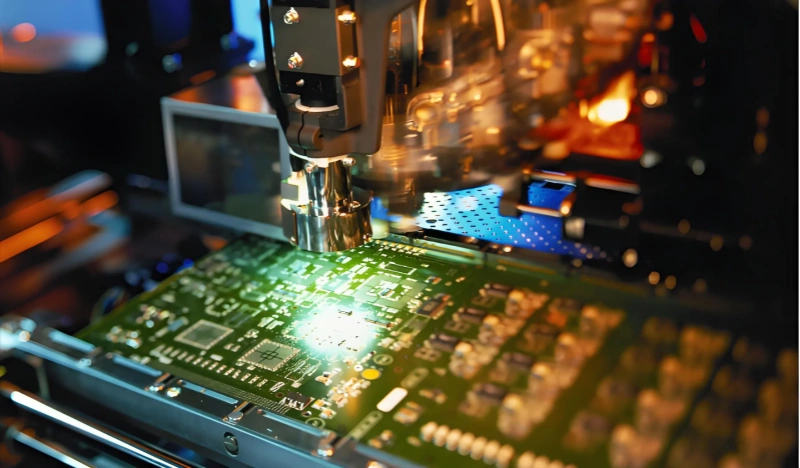
PCB surface finish is the metal connection between the bare copper on the board and the parts that solder to it. A PCB has a base copper surface. Without a protective coating, the base copper will oxidize easily. So we need a surface finish to protect the copper and to give a solderable surface for parts.
Surface finish is one of the most important steps in PCB manufacture and assembly. It has two main functions: one is to protect exposed copper traces, and the other is to provide a solderable surface so parts can be soldered to the PCB. The surface finish sits at the outermost layer of the PCB, above the copper, and acts like a coating over the copper.
Types of PCB Surface Finishes
1. Hot Air Solder Leveling (HASL)
Hot Air Solder Leveling (HASL) is one of the most common surface finishes in the industry. HASL comes in two main types: leaded and lead-free. It is also one of the cheapest surface finish options.
To form a HASL finish, the PCB is dipped into molten solder (tin/lead for leaded, or pure tin for lead-free). The solder covers all exposed copper on the board. After the board leaves the molten bath, high-pressure hot air knives blow across the surface to smooth the solder and remove excess material.
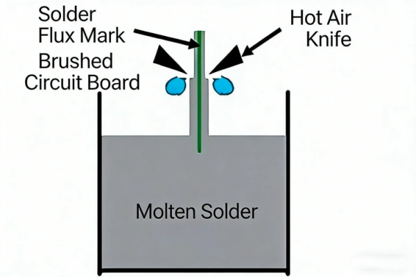
Key parameters to control in this process include solder temperature, air-knife temperature, air-knife pressure, dip time, and lift speed. HASL is widely used for SMT processes, but its rough surface limits use for fine-pitch applications or tactile switch contacts. High temperatures may cause copper dissolution, and it is less convenient for very thick or thin boards.
| Advantages | Disadvantages |
|---|---|
| Readily available | Uneven surface |
| Reworkable | Not good for fine pitch |
| Long shelf life | Contains lead (for leaded HASL) |
| Good solderability | Thermal shock risk |
| Low cost | Solder bridging |
| Large process window | Can clog or reduce plated through holes (PTH) |
| Longer storage time | Large thickness differences between big and small pads |
| Pads fully covered with solder before assembly | Not suitable for very fine-pitch SMD/BGA |
| Works for lead-free soldering | Not ideal for HDI products |
| Mature (supports visual/electrical inspection) | Not good for wire bonding |
2. Immersion Tin (ImSn)
Immersion Tin (ImSn) is formed by a chemical displacement reaction, depositing a tin layer directly on base copper. It protects copper during shelf life, and its tin-based composition matches common assembly solders.
Adding organic additives to the tin bath creates a granular tin layer, reducing tin whiskers/migration while improving thermal stability and solderability. It forms a flat copper-tin intermetallic, avoiding HASL’s flatness issues or excessive diffusion.
| Advantages | Disadvantages |
|---|---|
| Excellent flatness (ideal for SMT) | Process sensitive |
| Good for fine pitch, BGA, and small parts | Shorter shelf life (tin whiskers may appear after ~6 months) |
| Medium-cost, lead-free finish | Aggressive to solder mask |
| Good solderability after multiple thermal cycles | Not recommended with peelable masks |
| Compatible with horizontal production lines | Not suitable for tactile switch contacts |
| Suitable for fine geometry/lead-free assembly | Electrical testing needs special soft probe fixtures |
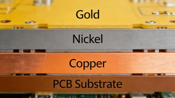
3. Electroless Nickel Immersion Gold (ENIG)
ENIG is a top choice for flat, fine-pitch, lead-free finishes. It is a two-step process: first depositing a thin electroless nickel layer (3–6 µm) as a barrier over copper, then an immersion gold layer (0.05–0.1 µm) to protect the nickel during storage.
The nickel layer is what parts actually solder to, while gold prevents nickel oxidation. Process steps include cleaning → etch → catalyst → electroless nickel → immersion gold → residue cleaning. Though effective, ENIG is complex and costly, with risks like “black pad” if uncontrolled.
| Advantages | Disadvantages |
|---|---|
| Flat surface | Expensive |
| Lead-free | Not easily reworked |
| Good for PTH | Risk of black pad defects |
| Long shelf life | Can cause RF signal loss |
| Complex process |
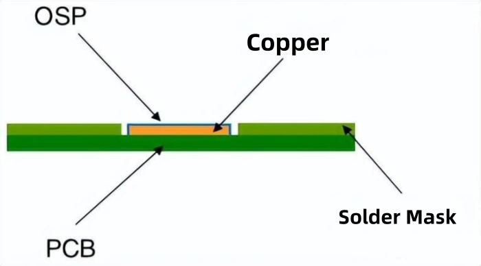
4. Organic Solderability Preservative (OSP)
OSP applies a thin organic film to exposed copper via a conveyor process, acting as a barrier against oxidation, thermal shock, and humidity. During soldering, flux removes the film to enable copper wetting with molten solder.
Typical steps: degrease → micro-etch → acid wash → pure water rinse → organic coating → rinse. OSP uses water-based compounds (no heavy metals), making it environmentally friendly.
| Advantages | Disadvantages |
|---|---|
| Flat surface | Hard to measure thickness |
| Simple process (smooth surface, good for lead-free SMT) | Not suitable for PTH |
| Reworkable (compatible with horizontal lines) | Short shelf life |
| Cost effective | May cause ICT issues |
| Environmentally friendly | Exposes bare copper at final assembly |
| Sensitive to handling | |
| Not suitable for >2 reflows | |
| Not for crimping/wire bonding | |
| Hard to inspect visually/electrically | |
| SMT may need nitrogen atmosphere |
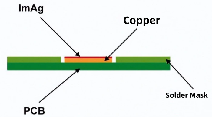
5. Immersion Silver (ImAg)
Immersion Silver is a non-electrolytic finish: the PCB is dipped into a silver ion bath, and a thin silver layer (5–18 microinches) replaces the copper surface. It is more eco-friendly than HASL/ENIG and cheaper than ENIG.
ImAg maintains good electrical performance/solderability even with heat/humidity exposure (though it may lose shine). It is sometimes paired with OSP to reduce silver sulfide tarnishing. Common uses include membrane switches, EMI shielding, aluminum wire bonding, and fine traces.
| Advantages | Disadvantages |
|---|---|
| Good solderability | Special storage required |
| Good surface flatness | Easy to contaminate |
| Low cost (RoHS compliant) | Short assembly window after unpacking |
| Suitable for aluminum wire bonding | Harder electrical testing |
6. Electroless Nickel Electroless Palladium Immersion Gold (ENEPIG)
ENEPIG forms a copper–nickel–palladium–gold stack (Ni: 3–6 µm; Pd: 0.1–0.5 µm; Au: 0.02–0.1 µm). The palladium layer (added vs. ENIG) protects nickel from corrosion and eliminates black pad risk.
It offers an extremely flat finish, supports multiple assembly cycles, and enables direct wire bonding. The thin gold layer is soft (prone to mechanical wear), but the underlying palladium maintains performance.
| Advantages | Disadvantages |
|---|---|
| Extremely flat surface | Still relatively costly |
| Lead-free | Reworkable but with limits |
| Good for multiple assembly cycles | Some process constraints |
| Excellent solder joints | |
| Supports wire bonding | |
| Low corrosion risk | |
| Long shelf life (≥12 months) | |
| No black pad risk |
7. Hard Gold (Electrolytic Hard Gold)
Hard gold is a gold layer (99.6% purity) plated over nickel, used in high-wear areas (e.g., edge fingers, connector contacts). A “soft gold” variant (99.9% purity) is used for wire bonding and high solderability (stronger joints than hard gold).
Electrolytic hard gold creates a durable surface, but it is costly and requires extra processing (e.g., masks/tapes, plating rails).
| Advantages | Disadvantages |
|---|---|
| Hard, durable surface | Very expensive |
| Lead-free | Extra processing/labor |
| Long shelf life | Requires masks/tapes |
| Needs plating/rails | |
| Can cause edge effects/etch back | |
| Not solderable above certain thickness | |
| May not fully encapsulate trace sidewalls (except fingers) |
How to Choose a PCB Surface Finish
Choosing a surface finish impacts yield, rework, field failure rate, testability, scrap rate, and cost. Key factors to consider:
- Pad flatness: Prioritize thin, uniform finishes (ENIG, ENEPIG, OSP) for flatness-dependent applications.
- Solderability/wetting: HASL offers strong wetting; OSP/ENEPIG may require adjustments.
- Wire bonding: Limit choices to ENIG/ENEPIG.
- Storage conditions: Avoid delicate finishes (e.g., OSP) if handling/storage is unregulated.
- Solder cycles: Choose rework-friendly finishes (HASL, OSP) for multiple reflows.
- RoHS compliance: Avoid leaded HASL if RoHS is required.
Conclusion
Select a surface finish that aligns with your board’s functional needs—each option has tradeoffs, but engineering adjustments can mitigate weaknesses (e.g., adjust solder alloy/preheat for OSP’s wetting issues).
This guide covers common PCB surface finishes and their process requirements. Feel free to request corrections or additional details.