Introduction
In PCB design and manufacturing, impedance control is a critical technical requirement. To understand its necessity, we first clarify the basic concept of impedance and then explore its types, impacts, and practical applications in PCBs.
1. What is impedance?
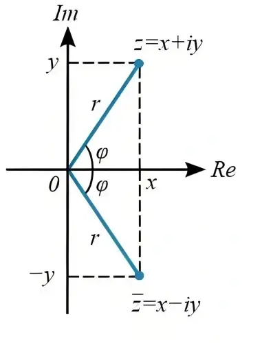
In a circuit that has resistance, inductance, and capacitance, the blocking effect these parts have on alternating current is called impedance. We write impedance as Z. Impedance is a complex number. The real part is resistance. The imaginary part is reactance. The formula is:Z = R + i(ωL − 1/(ωC))Here, the part that comes from capacitance and that blocks AC is called capacitive reactance. The part that comes from inductance and that blocks AC is called inductive reactance. Both types of reactance together are usually called just reactance.
2. Five types of impedance in PCB design and manufacturing
There are five types of impedance that people talk about when they design and make PCBs:
2.1 Characteristic impedance
In devices like computers and wireless communication gear, the energy that travels along PCB traces often comes as a square wave in voltage over time. People also call this a pulse. The resistance that the trace offers to that pulse is called the characteristic impedance. This is the impedance that matters for the path that carries a fast signal.
2.2 Differential impedance
If you drive two signals that are the same shape but opposite in polarity, you send them on two matched traces. At the receiver, the two signals are subtracted from each other. The impedance between these two traces is the differential impedance, often written as Zdiff.
2.3 Odd-mode impedance
This section explains odd-mode impedance as the impedance of one trace to ground when the two traces are behaving in a matched way. People sometimes call this Zoo. The two traces have the same value to ground in this condition.
2.4 Even-mode impedance
When the two signals have the same polarity at the drive end, the impedance of the two lines when tied together is called the even-mode impedance, written as Zcom.
2.5 Common-mode impedance
Common-mode impedance is the impedance of a single line to ground when both lines behave in the same way. People sometimes write this as Zoe. In many cases, common-mode impedance is larger than odd-mode impedance.
3. Why should PCB traces have impedance control?
PCB trace impedance is the combined effect of resistance and reactance. It blocks AC like any impedance does. In PCB production, controlling impedance is essential. Here are the main reasons:
3.1 Ensure normal conduction and signal transmission after component mounting
The board needs places to mount and plug in electronic parts. After parts are attached, we must make sure the board conducts well and that signals travel correctly. That is why designers often want impedance to be low where possible.
3.2 Production processes affect final impedance
PCB boards go through many steps during production. These steps include copper plating, tin plating (or chemical plating or hot-dip tinning), and soldering of connectors. The materials used in these steps must have low resistivity so that the board’s final impedance meets product requirements and the board can work normally.
3.3 Tin plating is a key factor affecting impedance
The tin plating on a PCB is one place where problems happen most easily. It is a key step that affects impedance. The biggest issues with chemical tin plating are that it discolors easily (it can oxidize or absorb moisture), and that it has poor solderability. These problems make the board hard to solder, raise the impedance, reduce conductivity, and make overall board performance less stable.
3.4 High-frequency signals require strict impedance control
A PCB trace carries many different signals. If you need higher transmission speed and so you raise the signal frequency, small differences in trace etching, stackup thickness, or trace width will change the impedance. This change can cause signal distortion and reduce the board’s performance. Therefore, you must keep the impedance within a controlled range.
4. What impedance means to the PCB industry
For people in electronics, impedance is closely related to the reliability and performance of PCBs, especially in terms of tin plating layers:
4.1 Weaknesses of chemical tin plating layers
The weakest part of a chemical tin plating layer is that it changes color easily, which means it oxidizes or absorbs moisture. It also has poor solderability, leads to high impedance, causes poor conductivity, and makes the whole board’s performance unstable. Tin plating can also grow tin whiskers. Whiskers can short traces and can cause burning or fire in extreme cases.
4.2 Role of tin plating in current transmission
The main copper traces on a PCB are copper foil. The solderable points on that copper foil are the tin plating layers. Electronic parts attach to the tin plating layer with solder paste or solder wire. When the solder melts during reflow, the material that joins the electronic part to the tin plating is metallic tin, which is a good electrical conductor. So we can say simply that the electronic part connects to the copper foil on the PCB through the tin plating layer. This means the purity and the impedance of the tin plating layer matter a lot.
4.3 Tin plating’s role in impedance testing
Before parts are mounted, when we measure impedance with a test tool, the test probe touches the tin plating layer on the board surface and then connects to the copper foil under the tin. This shows that the tin plating layer is a key part for current flow. It is the key factor that affects impedance and the board’s overall performance. It is also a part that people often overlook.
4.4 Impact of tin compounds on impedance
Outside the pure metal of tin, compound forms and mixtures are poor conductors or even nonconductors. This is also why distributed capacitance or stray capacitance appears in a circuit. If the tin plating layer contains these tin compounds or mixed areas that seem partly conductive but are not good conductors, then the current resistivity now or the resistivity that will form after future oxidation or moisture-driven electrochemical reactions will be high. That high resistivity and the related impedance can affect logic levels and signal transmission in digital circuits. At the same time, the characteristic impedance along a trace may not be consistent. These problems will affect board function and device performance.
4.5 Hidden and variable impedance issues
In short, the material and the condition of the plating on the PCB are the main and most direct reasons that affect the board’s characteristic impedance. Because the plating can age and change with humidity and electrochemical effects, the impedance problems can become hidden and changeable. The reason they hide is twofold: first, you often cannot see the change with the naked eye; second, you cannot continually measure it because the plating changes over time and with humidity. That makes the issue easy to miss.
5. The ideal model for impedance matching
Radio frequency engineers often meet the problem of matching impedance. Put in simple terms, the aim of impedance matching is to make sure that a signal or energy moves efficiently from the source to the load.
The ideal model is this: we want the source output impedance to be 50 ohms, the transmission line to have 50 ohms, and the load input impedance to be 50 ohms. If the whole path is 50 ohms from start to end, that is the best case.
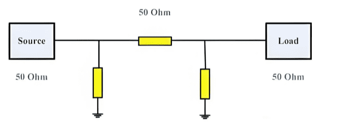
But in real life, the source impedance is not always 50 ohms, and the load impedance is not always 50 ohms. When that happens, we need one or more impedance matching circuits.
Matching circuits are made from inductors and capacitors. Then we use capacitors and inductors to tune the matching network so that the RF performance is best.
6. How to do impedance matching
There are two main ways to match impedance. One way is to change the impedance value with components. The other way is to change the transmission line.
6.1 Change impedance with components
To change the impedance with parts, we use capacitors and inductors in series or in parallel with the load. This adjusts the load impedance so it better matches the source.
6.2 Change the transmission line
To change the transmission line, we change the distance or the physical path between the source and the load. We can then pair that line change with capacitors and inductors to make the net impedance seen by the source zero. When the net reflected impedance is zero, the signal will not reflect back. All the energy will be absorbed by the load.
7. Common design targets for high-speed PCB traces
For high-speed PCB work, the common choices are:
- Single-ended digital traces are usually designed to be 50 ohms.
- Coaxial cable baseband is usually 50 ohms.
- For some band applications, 75 ohms is a common design.
- Twisted pairs for differential signals are usually designed between 85 and 100 ohms.
8. Final notes and simple rules to remember
- Impedance affects how well a trace carries a fast signal. Keep it controlled to avoid signal loss and distortion.
- The plating and surface finish on the board can change impedance over time and with moisture. Pick the right finish and control the process to keep impedance stable.
- When the source and load do not match, use matching circuits made of capacitors and inductors or tune the line length to reduce reflections.
- For digital signals, aim for standard trace impedances such as 50 ohms for single-ended lines and 85–100 ohms for differential pairs.