Introduction
To design a successful flexible PCB, designers need a solid grasp of the core flexible-board requirements. This article explains important design rules and practical details. Flexible PCBs were first used in the military, but today they appear across nearly every industry. Below are ten key points every designer should consider.
The 10 Key Design Requirements
- Prerequisites for flexible design
- Drawings must define the rigid-to-flex interface
- Flexible PCB stackup and layer order
- Descriptive notes for the PCB manufacturer
- Flexibility and bend radius
- Dimensional stability
- Shielding requirements
- Drill symbol table
- (Practical design do’s & don’ts)
- FPC soldering processes and controls

Design Considerations for Flexible PCBs
1 — Prerequisites for flexible design
Start the design by specifying several board elements. These must be included on the drawing or in the documentation:
- Number of layers
- Final board thickness
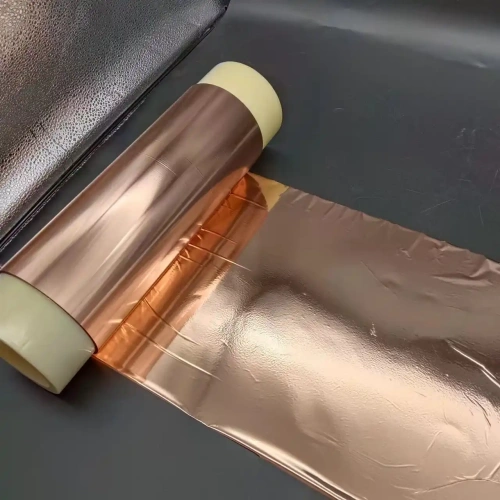
- PCB base/flexible material(s) (e.g., polyimide types)
- Surface finish (HASL, ENIG, etc.)
- Drill sizes (finished hole diameters)
- Plated thru-holes (if any)
These items may seem obvious, but they are sometimes missed. Missing information forces the manufacturer to ask follow-up questions and can delay turn-around time.
2 — Drawings must define the rigid-to-flex interface
The dimensioned drawing carries many critical design measurements. It must clearly show the rigid-to-flex interface and exactly where the two material types meet. Typical board outline tolerance is ±0.010 in (±0.25 mm) unless otherwise specified.
A flexible PCB drawing should also show:
- Location and size of stiffeners (rigidizing elements)
- Thickness and material for each section of the board
- Whether the flex area is static or dynamic (see below)
- Areas that rarely bend versus areas that bend often
Static vs. dynamic flex: PCBs that may be bent up to ~20 times are usually considered semi-static. Boards that bend repeatedly during operation are dynamic flex (for example, the moving parts inside a printer). Mark dynamic flex zones clearly on the drawing.
3 — Flexible PCB stackup and layer order
The stackup distinguishes rigid layers from flexible layers. A good stackup drawing lists the thickness of every layer and the copper weight for conductive layers. It should also specify impedance traces and target values (for example, 50 Ω or 100 Ω differential), when needed for signal integrity.
4 — Descriptive notes for the PCB manufacturer
Provide clear notes for the manufacturer covering items such as:
- Class or grade (Grade 1, 2, 3), connector/wiring types, and mounting requirements
- Type of flex copper-clad material used (e.g., polyimide with specific copper cling)
- Coverlay / covercoat material and type (material that covers flex copper)
- Maximum overall board thickness
- Minimum size for plated thru-holes
- Electrical test requirements (e.g., 100% electrical test, flying probe)
- Coverlay/solder mask color and silkscreen color
- Board markings: part number, revision, logo, serial number, etc.
- Packaging and shipping instructions
Well-written notes reduce misunderstandings and speed manufacturing.
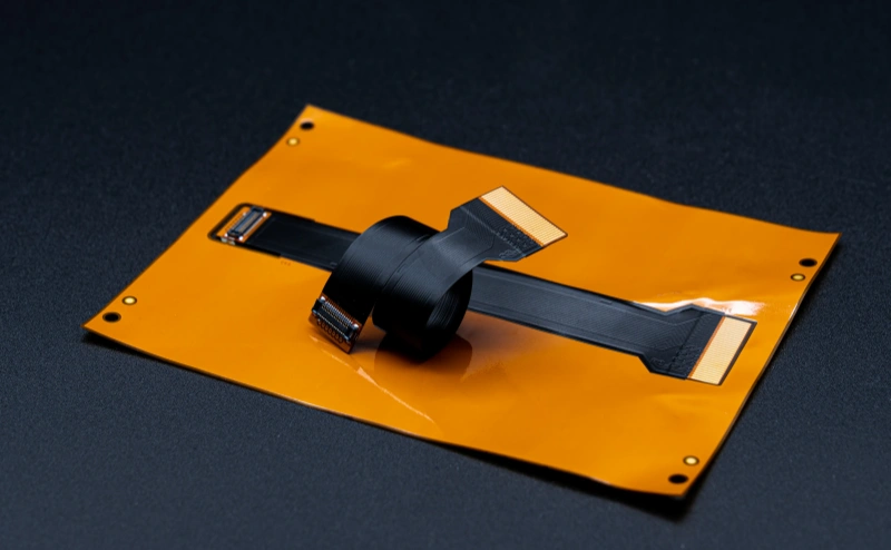
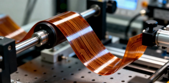
5 — Flexibility and bend radius
The flexibility of an FPC depends mainly on the materials and the bend radius. The bend radius is the smallest radius the flex area can bend without damage.
It’s essential to know how many times the board will bend during normal use. If the circuit bends more often than designed, copper traces can stretch and eventually crack.
- Boards bent up to about 20 times are typically semi-static.
- Boards that bend repeatedly in normal operation are dynamic flex and require special materials and design treatment. Printers commonly use dynamic flex circuits.
Bend radius also depends on the number of layers and the types of materials used in the flex region. When in doubt, design with a larger radius and lower copper density in bend zones.
6 — Dimensional stability
Dimensional stability is critical for high-density designs. Small dimensional shifts can occur during processing (etching, plating, pressing, heat, chemicals). Designers should expect these shifts and plan part numbering and fabrication accordingly.
Implement scaling factors
During processes such as heat lamination, panels may undergo size changes. Designers and manufacturers use scale factors and measured process data to predict percentage losses and to enlarge artwork or drill patterns accordingly. These calculations are done dynamically and are essential when finalizing drill programs for multilayer boards.
Software compensation
Use software-controlled measurements and optical fiducials to analyze dimensional shifts. Panel fiducials, corner targets, and iterative measurements let manufacturers perform X, Y and theta corrections to align layers correctly.
7 — Shielding requirements
Shielding is often necessary for flexible circuits to limit EMI and ESD and to preserve controlled impedance. Typical shielding solutions include:
- Copper cladding or foil
- Copper hatched patterns (shadowing)
- Silver paste or conductive epoxy
- EMI thermoplastic shielding films
Choose a shielding method that meets your EMI/ESD and impedance control goals.
8 — Drill symbol table
A drill symbol table lists every finished hole size and tolerance used on the PCB. It is a concise reference for all hole types on the board.
Practical Design Do’s & Don’ts for Flex Zones
- Avoid placing vias inside bend areas. If vias are necessary, locate them in flat, non-bending sections.
- Route lines as curved traces through bend zones rather than with sharp corners.
- Avoid sudden changes in trace width in the bend area. Smooth transitions are more durable.
- Maintain a minimum clearance of 20 mils (0.020 in / 0.5 mm) between copper annular rings and the nearest via or pad where possible.
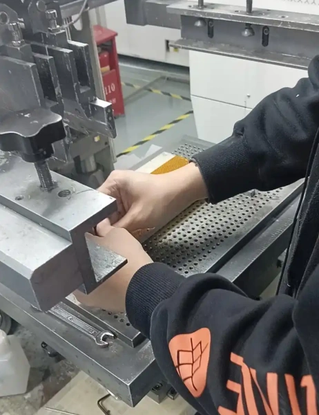
Common FPC Soldering Practices (Hand Soldering vs. Press Soldering)
Today, two common soldering methods for flexible circuits are used: (1) solder press (reflow or press-fit soldering) and (2) manual hand soldering. We recommend solder press machines when possible because they produce more consistent joints with fewer cold joints and shorts. The downside is higher equipment cost and some layout constraints. Below we summarize recommended manual soldering practice for FPCs.
Hand soldering process (recommended tools and flow)
Hand soldering is done with a soldering iron and solder wire. For FPC work, we recommend a quality temperature-controlled iron (OKi brand is commonly used in industry examples) and suitable solder wire.
Typical process flow:
- FPC placement and alignment
- Solder deposition and soldering (hand soldering)
- Visual inspection
- Electrical testing
Before soldering (alignment):
- Check that FPC pads and the mating solder surface are clean and flat, and not oxidized.
- After placement, leave about 1.00 mm of exposed tail on the pad area so that solder can properly wet the joint.
Key controls used in our shop
- Pre-heat time: Place the iron tip on the pad for 2–3 seconds before applying solder. This ensures the pad and FPC area are hot and helps prevent cold joints.
- Iron angle: Tilt the iron relative to the gold finger at about 30° for good access and control.
Four main controls during soldering:
- Time: A guideline is roughly 3 seconds per iron-tip length, total time typically between 4–10 seconds depending on joint size.
- Temperature: Typical iron temperature range 290–310 °C for leaded solder; adjust for your solder alloy and pad size.
- Solder feed point: Feed solder slightly ahead of the iron tip toward the pad for best wetting.
- Pressure: Light pressure from the iron tip is acceptable, but avoid pressing hard enough to damage gold fingers or pads.
These are general guidelines. Adjust them to match your solder alloy (lead-free requires higher temperatures), pad geometry, and assembly equipment.