Introduction
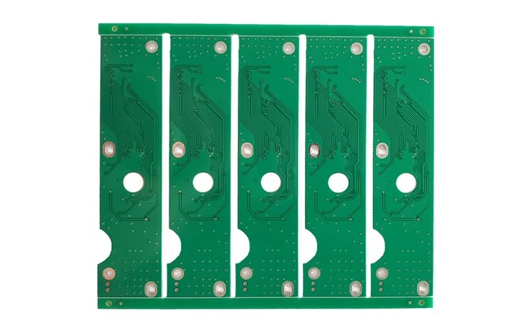
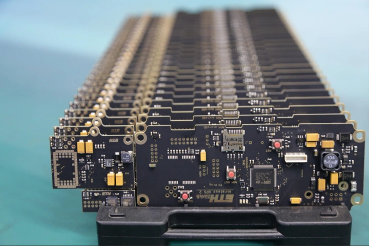
Printed circuit boards (PCBs) are one of the most important parts of an electronic circuit, and they affect how the device works. Knowing how a PCB is made helps you design it well and pick the right maker. In industry, about 60% of PCBs are multilayer. Demand for smaller, faster, and stronger devices drives the need for multilayer PCBs. These boards use copper as the conductor, and copper helps them carry current. This article explains how multilayer PCBs are made and gives simple guidance on how to choose a copper multilayer PCB manufacturer.
A Short View of Multilayer PCB Manufacturing
In broad terms, the manufacturing steps that copper multilayer PCB makers follow are straightforward. The process goes like this:
- Choose the materials for the inner core, the prepreg sheets, and the copper (Cu) foil.
- The prepreg sheet is made of glass cloth and epoxy resin.
- The core board is covered with copper foil of a chosen weight and thickness.
- Cover these stacks with a light-sensitive dry film. Then expose the film with ultraviolet (UV) light and the photoresist. The internal circuit data transfers to the resist by using UV light.
This sequence prepares a core laminate. But a multilayer PCB is made by laminating many such layers. Below we look at the multilayer lamination process so you can fully grasp how multilayer PCBs are built.
Understand the Multilayer Lamination Process
Multilayer lamination is a step-by-step process. The base of a layered board is a copper foil sheet with one layer of prepreg on it. The number of prepreg layers changes with what the board needs. Then a core is placed on the prepreg sheet, and more prepreg sheets with copper foil cover that core. This builds one laminated section of the multilayer PCB stack.
You stack the same laminate sections on top of each other. After you add the final copper foils, you create the final stack, which people call a “book.” Each laminated section inside the book is called a “chapter.”
After the book is ready, you move it to a hydraulic press. The press heats the book and applies strong pressure and vacuum. This step is called curing because it makes the laminated layers bond and it lets the resin in the prepreg flow and fuse with the core and foil layers. After curing, you take the assembly out and let it cool at room temperature. As the resin settles and hardens, the copper multilayer PCB is formed.
Even though most copper multilayer PCB makers follow the same main steps, the final result depends on careful control of many details. That is why it is important to work with a good multilayer copper PCB manufacturer.
Materials and Key Parts in the Process
Inner Core
The inner core is a rigid sheet that already has copper on one or both sides. It forms the central electrical layer or layers of the board. The core gives the stack its main thickness and base copper pattern.
Prepreg
Prepreg is a sheet made of woven glass cloth soaked in epoxy resin. Prepreg acts as the adhesive and dielectric between cores. When heated under pressure, the resin flows and bonds the layers.
Copper Foil (Cu Foil)
Copper foil is the conductive material. It comes in different weights and thicknesses. The choice of copper thickness affects current capacity and trace design.
Dry-Film Photoresist
The laminates are covered with a light-sensitive dry film. When you expose the film to UV light, the internal circuit pattern transfers to the film. This step lets you make the inner copper circuit by etching the exposed areas.
Curing Equipment (Hydraulic Press)
The hydraulic press provides heat, pressure, and vacuum. These forces cure the resin in the prepreg and fuse the stack into a single solid part.
How the Inner Circuit Image Is Made
For inner layers, the circuit image is transferred to the dry-film photoresist. The usual steps are:
- Place the dry film on the copper surface.
- Put a mask or film with the inner layer pattern over the dry film.
- Use UV light to expose the pattern. The light hardens the photoresist where you want the copper to stay.
- Develop the photoresist so the unexposed parts wash away.
- Etch the exposed copper away. The remaining copper matches the inner circuit pattern.
This process gives you the inner copper traces inside the core laminate.
How to Build the Multilayer Stack in Order
The stack build follows a plan. A typical multilayer stack plan may look like this:
- Start with a core that has inner copper traces.
- Add a sheet of prepreg over the core.
- Add another core or prepreg with copper foil as needed.
- Repeat the layers until you reach the desired layer count.
- Add a final outer copper foil on the top and bottom.
- Make a full book by stacking multiple laminates and final foils.
After the stacked book is complete, place it in the hydraulic press. Apply the preset heat and pressure cycle and hold it for the set time. The resin melts and flows, and the layers bond into a single unit. The vacuum helps remove trapped air and stops voids from forming. After curing, cool the board slowly so the resin settles and the lamination stays stable.
Why Layer Order and Prepreg Count Matter
The number of prepreg sheets and their order control the final board thickness and dielectric spacing. The layer order also sets where traces and power planes sit in the board. When you design a multilayer board, you must pick the stackup carefully because it affects signal integrity, impedance, and thermal behavior. The right stack helps you control impedance and reduce noise. It also helps your board handle heat and current.
Why Attention to Detail Matters
Although the main steps are clear, making a reliable multilayer board needs close control of many small things. These include:
- Choosing the right prepreg type and weight.
- Matching copper thickness to current needs.
- Controlling the press temperature, pressure, and time.
- Using the right vacuum level to remove air.
- Aligning inner layers so vias and pads line up.
- Controlling resin flow so no voids form.
- Choosing the right etch and develop parameters for inner layers.
Poor control in any of these areas can cause delamination, voids, misaligned layers, or poor electrical performance. For this reason, choose a maker who follows strict quality control and who knows how to handle precise multilayer work.
How to Choose a Good Multilayer PCB Manufacturer
When you pick a multilayer PCB maker, consider several factors. These simple points will help you make a better choice.
Technical Capability
This process needs trained operators, the right machines, and the right controls. A reputable multilayer copper PCB maker will have trained staff and proper equipment.
Experience
Check the maker’s experience before you decide. You can learn this from their website or ask in talks. Check their experience in your industry and the kinds of projects they have done.
Custom Options
Some devices use standard board sizes, but many need custom sizes and special layer counts. Make sure your chosen maker can make boards to your custom specs.
Industry-Specific Certifications
If you are in a critical field such as medical, military, aerospace, or aviation, certifications matter a lot. These fields need certified processes and traceable records. Check whether the manufacturer has the right certifications for your industry.
Process Control and QA
Ask about their quality checks, layer alignment methods, and void detection. See if they run regular process audits and keep records of their process parameters.
Material Sourcing and Traceability
Good makers know their material sources and can show traceability for prepreg, copper, and cores. This traceability matters if you need certified materials.
Lead Time and Cost Balance
A lower price is fine for some projects, but for complex multilayer boards you may need a maker who balances cost with quality and lead time. For prototypes, find a maker who can handle small batches fast. For larger runs, consider a maker with stable production capacity.
Communication and Support
Clear communication is simple but essential. Your maker should guide you on stackup choices, impedance control, and design for manufacturability. They should answer questions and offer practical advice.
Final Notes and a Mention of Philifast
Multilayer PCB making is a layered and careful process. You pick materials, build stacks, expose inner circuits, and cure the whole stack in a press. Good results come when makers control the small steps well. For that reason, picking the right multilayer copper PCB manufacturer is important.
If you are looking for a partner, check their technical skills, experience, custom options, certifications, and quality systems. In the text above, we also mentioned our company, Philifast, which is a PCB manufacturer with experience in multilayer copper PCB production.