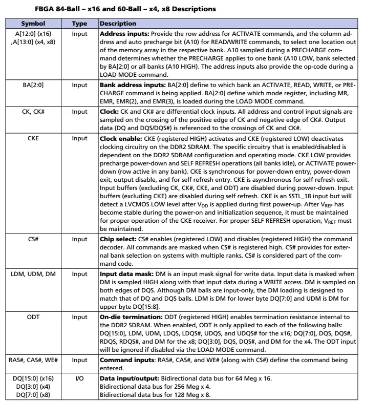
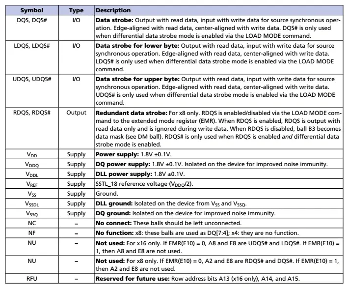
1. Layout
Component placement — ten rules
- Follow the rule “place large before small, place hard before easy.” Important circuit blocks and key parts should be placed first.
- Use the schematic block diagram as a guide. Place main parts to match the board’s main signal flow.
- Arrange parts so testing and repair are easy. Do not put large parts next to small parts that need access. Leave enough space around parts that need testing or adjustment.
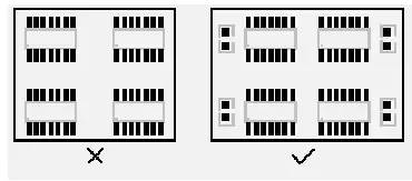
- For repeated circuit blocks, use a symmetric layout when possible. Symmetry helps repeatability and testing.
- Optimize the layout by even distribution, balance of center of gravity, and neat board look.
- Place the same type of through-hole parts in the same X or Y direction. For polarized discrete parts of the same type, keep their orientation consistent in X or Y for easier assembly and inspection.
- Spread heat-generating parts across the board so the board and the final product cool better. Put temperature-sensitive parts away from hot parts. Do not place sensors for temperature next to hot components, except when the sensor must measure that heat.
- Try to meet these wiring needs: keep total trace length short, make key signal traces the shortest. Keep high-voltage or high-current traces well apart from low-voltage or low-current weak signals. Separate analog signals from digital signals. Keep high-frequency signals away from low-frequency signals. Give enough spacing around high-frequency parts.
- Place decoupling capacitors as close as possible to the IC power pins. Make the loop that goes from power to capacitor to ground as short as possible.
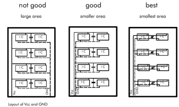
- When placing parts, try to put parts that use the same power rail close together. This makes later power partitioning easier.
2. Routing (Traces)
(A) Routing priority
- Key signals first: route critical traces like small analog signals, high-speed lines, clock signals, and synchronous lines before others.
- Density first: start routing in the area with the most complex connections on the board. Begin from the most crowded region.
Notes:
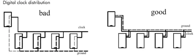
a. Give clock, high-speed, and sensitive signals dedicated routing layers when you can. Make their return loop area as small as possible. If needed, route these by hand first, use shields, or increase clearance to protect signal quality.
b. Avoid placing interference-sensitive signals where the EMC environment is bad, such as between power and ground planes.
c. For nets that require controlled impedance, follow required trace width and length rules.
(B) Four common trace styles
1. Clock routing
Clock traces are one of the biggest sources of EMC problems. On clock lines, minimize vias. Avoid routing clock lines in parallel with other signals. Keep them apart from general signals to reduce interference. Also, keep clock lines away from power areas to avoid cross coupling between power and clock.
If there is a dedicated clock generator chip on the board, do not route traces under it. Fill copper under that chip, and if needed, cut the plane specially for it. Many chips use a reference crystal oscillator. Do not route under the crystal. Fill copper under the crystal to isolate it.
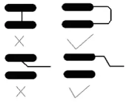
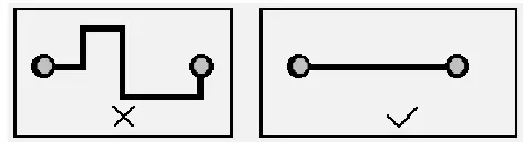
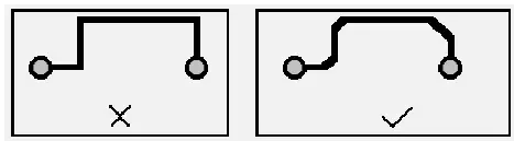
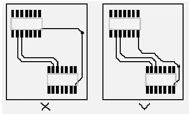
2. Right-angle traces
Right-angle traces are normally avoided in PCB routing. They are a common measure of routing quality. A right-angle can change the trace width effectively. This change causes an impedance discontinuity. Not only right angles, but sharp corners and acute angles can also change impedance.
The main effects of right-angle corners on signals are:
- The corner acts like a capacitive load on the trace. This slows down the rise time.
- Impedance discontinuity can cause signal reflection.
- The sharp corner tip can generate EMI.
So avoid right angles and sharp corners in high-speed or sensitive traces.
3. Differential pairs
See reference: Altium Designer — Differential routing and impedance matching.
Differential signals are widely used in high-speed circuits. The key signals in many designs use differential pairs. In simple terms, the driver sends two equal and opposite signals. The receiver reads the difference between the two voltages to decide if the logic is “0” or “1.” The two traces that carry a differential signal are the differential pair.
Compared to single-ended traces, differential pairs have clear advantages:
a. Better noise immunity. The two traces are strongly coupled. External noise couples to both traces almost the same way. The receiver looks at the difference, so common-mode noise is canceled.
b. Lower EMI. Because the two signals are opposite, their radiated fields cancel. The closer they are, the more the fields cancel and the less energy radiates.
c. Better timing accuracy. The switching edge is at the crossing point of the two waveforms. This reduces sensitivity to process and temperature, so timing error is lower. Differential signaling is good for low-amplitude signals. LVDS (Low Voltage Differential Signaling) is an example of small-amplitude differential signaling.
To get these benefits in routing, PCB engineers follow two main rules: “equal length and equal spacing.”
- Equal length keeps the two signals in opposite phase and reduces common-mode error.
- Equal spacing keeps the differential impedance constant and reduces reflections.
Sometimes a rule “keep the pair close” is also used.
4. Serpentine (meander) traces
Serpentine traces are used to adjust delay and meet timing requirements. Designers must know that serpentine traces degrade signal quality and change transmission delay. Try to avoid them when possible. But in practice, to meet setup and hold time or reduce skew in a signal group, serpentine traces are often necessary.
Notes:
- For differential pairs, run the two traces in parallel and minimize vias. If you must use vias, use them as pairs so impedance stays balanced.
- Keep bus traces with the same function routed side by side and make their lengths as equal as possible. Place vias that come from SMT pads a bit away from the pad.
(C) Common routing rules
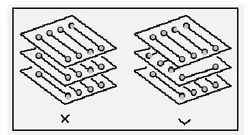
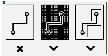
1. Direction control
Make sure traces on adjacent layers run orthogonally. Avoid routing the same direction on adjacent layers to reduce layer-to-layer crosstalk. If you can’t avoid same-direction routing because of board structure, use a ground plane to isolate the layers or add grounded traces between signal traces.
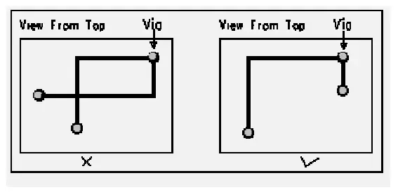
2. Open-loop check
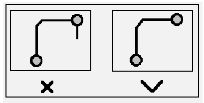
Do not leave traces with one end floating (dangling). A dangling line can act like an antenna and cause unwanted radiation or reception.
3. Impedance control
Keep the same line width in the same net. Changes in width change characteristic impedance and can cause reflection on high-speed lines. If you must change width, keep the inconsistent parts as short as possible.
4. Length control
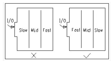
Keep traces short to reduce interference from long traces. For important lines like clocks, place the oscillator near the device that uses the clock. For a driver that drives many devices, pick the network topology by the system needs.
5. Corner rule
Avoid sharp and right-angle corners to reduce unwanted radiation and to meet manufacturing limits.
6. Decoupling rule
A. Add needed decoupling capacitors on the PCB to filter noise on the power rails. This helps power stability. On multilayer boards the exact decoupling locations are less strict, but on double-layer boards the layout and power routing to decoupling caps directly affect system stability and can decide success or failure.B. On double-layer boards, route the power through the filter caps before powering parts.C. In high-speed designs, correct decoupling is critical to board stability.
7. Zoning and layering rule
A. Place different frequency blocks apart to avoid mutual interference and to shorten high-frequency paths.B. For mixed-signal boards, place analog and digital circuits on separate sides or areas, and use a ground plane between routing layers to isolate them.
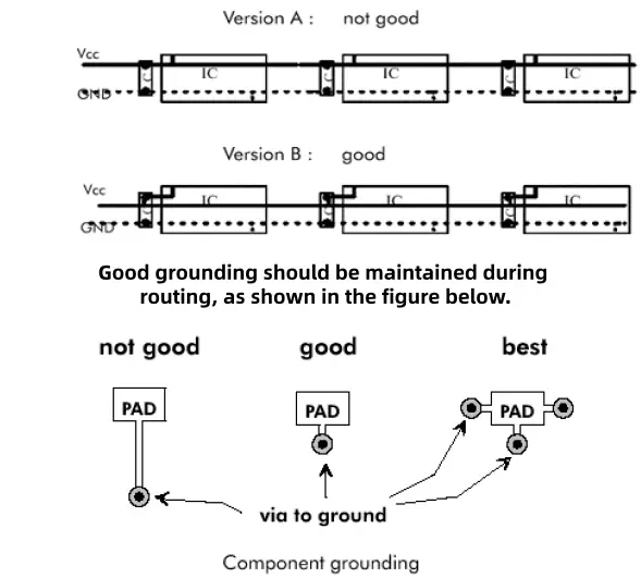
8. Ground return loop rule
Keep the signal trace and its return loop area as small as possible. Smaller loops radiate less and pick up less interference.
9. Power and plane integrity
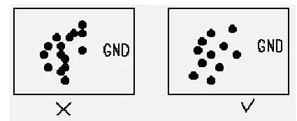
In areas with many vias, avoid making holes that cut power or ground planes into isolated islands. Plane cuts can break plane integrity and increase return loop area. This increases noise and radiated emission.
10. 3W rule for spacing
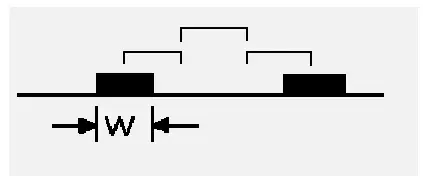
To reduce crosstalk, keep trace center-to-center spacing at least 3 times the trace width (3W). This keeps about 70% of the field from coupling. To get about 98% isolation, use 10W spacing.
11. Shielding
For very important signals like clocks or sync lines, reduce loop area by shielding. Use ground traces around the signal or use shielded copper cables for extreme cases. Make sure the shield ties well to the ground plane.
12. Termination rules
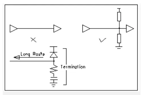
In high-speed digital circuits, when trace delay is greater than one quarter of the signal rise time, the trace must be treated as a transmission line. Match the input and output impedance of the driver to the line. There are many matching schemes, and the choice depends on topology and routing.A. For point-to-point links (one driver, one receiver), choose series termination at the source or parallel termination at the load. Series termination is simple and cheap but can add delay. Parallel termination matches well but is more complex and costly.B. For one driver to many receivers (point-to-multipoint), if the network is a daisy chain, use parallel termination at the end. If it is a star network, follow point-to-point rules. Balance cost, power, and performance when choosing. Full match is not always practical; limit reflections to acceptable levels.
13. Closed-loop checks
Prevent signals forming self-loops across layers. Multilayer boards can create self-loops that cause radiation.
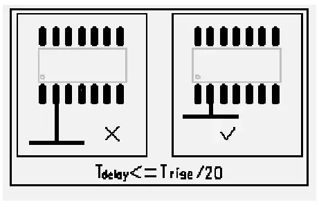
14. Branch length control
Keep branch lengths short. Typical rule: Tdelay ≤ Trise / 20.
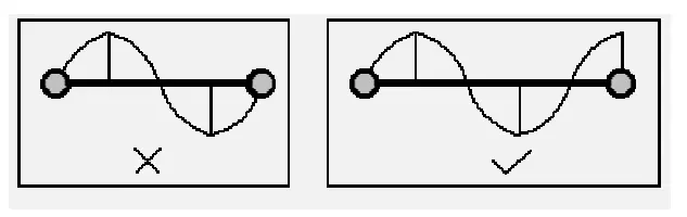
15. Resonance rule
For high-frequency signals, avoid trace lengths that are integer multiples of the signal wavelength, which could cause resonance.
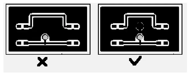
16. Isolated copper area control
Isolated copper areas can cause uncertain problems. Tie isolated copper to a ground net or remove it to improve signal quality. Some manufacturers add copper in empty regions to help manufacturing and to reduce board warp.
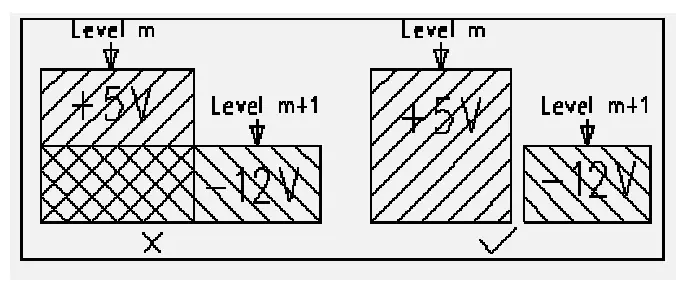
17. Overlapping power plane rule
Avoid overlapping different power planes in space. This reduces interference between supplies with large voltage differences. If overlap cannot be avoided, consider adding an isolation ground plane between them.
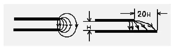
18. 20H rule for edge effect
The electric field between power and ground planes can radiate at the board edge. To reduce this, shrink the power plane inward from the board edge. If you shrink the plane by 20 times the dielectric thickness (20H), you can limit about 70% of the field inside the ground plane edge. Shrinking by 100H can limit about 98%.
(D) Other routing notes
- For single- and double-layer boards, make power traces wide and short. A typical rule: 1 mm trace width can carry about 1 A; use this to size power and ground traces. Keep power/ground loop area small.
- If a power trace is long, its coupled noise can go directly into the load. Decouple power to each load before the load input. For each load, use independent decoupling and filter the rail before entering the load to reduce mutual interference.
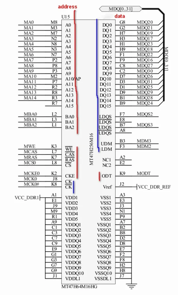
3. DDR Routing Rules
See references: DDR routing rules and process; DDR2-800 and DDR3 signal integrity design; DDR2 routing rules parts one and two.
(A) Understand DDR2 signals first
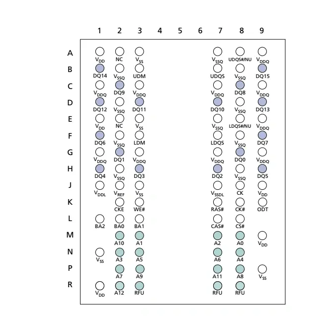
Example used here: DDR2 chip MT47H64M16HG.
Packing and pinout details (package, pin definitions, and schematics) are important in layout and routing. Know the signal groups: data lines and address lines.
Signal groups
- Data: DQ[0–15], DQS, DM, and clock CK/CK#.
- Address: A[0–15], BA[0–2], and control signals CS, WE, RAS, CAS. Also CKE and ODT.
For DDR routing, follow the specific rules that match the chip and the memory system topology. Some general DDR routing points are:
- Keep data strobes (DQS) close to data (DQ). Tie timing so that DQS meets setup and hold at each receiver.
- For point-to-point or fly-by routing of address and command lines, pick the topology recommended by the memory vendor. Fly-by routing often needs termination near the end of the line.
- Route address and command traces with controlled impedance and matched lengths where required.
- For multi-bit busses, match matched lengths on each group. Keep groups separate by function.
- Avoid stubs and use proper termination to reduce reflections.
- Keep power and ground planes continuous and place decoupling close to the memory and controller power pins.
- Place the memory chip and controller so that the critical high-speed paths are short and have minimal layer transitions.
(For more exact DDR layout choices, follow the memory vendor’s application notes and the board’s signal integrity analysis.)
4. Closing notes
- Always check your layout with the schematic and the block diagram. Place main parts first. Then route critical signals. Then finish other routing.
- For high-speed and mixed-signal designs, plan layer stack-up, plane placement, and return paths early. Use controlled impedance and signal isolation where needed.
- Use basic rules: short loops, matched lengths for critical groups, stable power, and good decoupling. These rules improve signal quality and reduce EMI.
- When in doubt, follow vendor application notes for DDR, high-speed transceivers, and special interfaces.