PCB or printed circuit board is the quiet hero in modern electronics. Most users do not know how the parts inside the devices they use work together. But for engineers, OEMs, and designers, there is a lot to learn about PCBs.
This guide aims to help both new and experienced engineers make better design choices early. Better choices lead to better parts for the final product.
Let’s start with the basics.
What is a PCB?
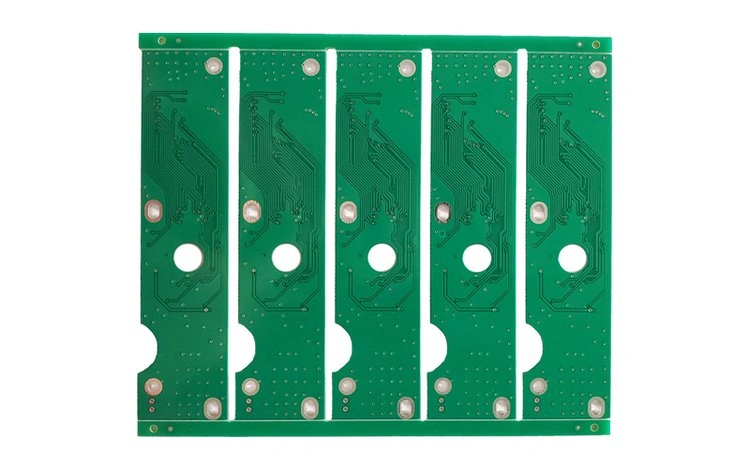
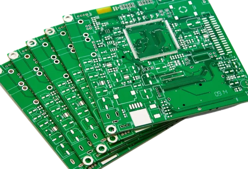
A printed circuit board (PCB) is the core of any electronic device. It has two main jobs: hold electronic parts and connect those parts so they work together.The board is made from a non-conductive base material, like fiberglass. One or both sides of that base are covered with copper. The copper makes the electrical paths. The unused copper is etched away. The remaining copper forms the traces that connect parts.
PCB, PCBA, PCA — what is the right name?
People in the industry use many acronyms for printed circuit boards. It can be confusing. The key terms are:
- PWB — Printed Wiring Board. An older name used when connections were mainly point-to-point.
- PCB — Printed Circuit Board. Technically this means the etched board before parts are mounted. The term PCB became the official name for the bare board in 1999.
- PCA — Printed Circuit Assembly. This term was used after the 1999 change to be clearer.
- PCBA — Printed Circuit Board Assembly. This is a PCB with all its parts mounted.
When people speak about the finished, assembled board, they often say “PCB” in everyday talk. When you talk to manufacturers or suppliers, be clear if you mean the bare board (PCB) or the assembled board (PCBA).
How does a PCB work?
A PCBA acts as a central hub that ties all electronic parts in a device together. Boards can be made in multiple layers. Conductive paths are placed on or inside the base material. These copper traces carry electricity and form the circuits. Parts are soldered to the board so the device works. The board also insulates and guides current safely.
What parts make up a PCB?
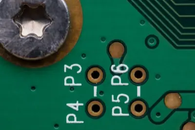
Each PCB hardware part plays a vital role in powering an electronic device. Basic PCB parts include traces, pads, vias, copper planes, solder mask, and silkscreen. (For layout or visual summary, a simple diagram is helpful.)
What is a PCB made of?
A board is made from four key items:
- Substrate — the base of the PCB. Usually fiberglass or another non-conductive material. The board can be single-layer or multi-layer.
- Copper — used to carry current. Copper on the PCB replaces many wires.
- Solder mask — the layer that protects the board and helps form the connections between the board and parts. The solder mask also protects the traces below from damage.
- Silkscreen — used to mark part locations, warnings, and other board features.
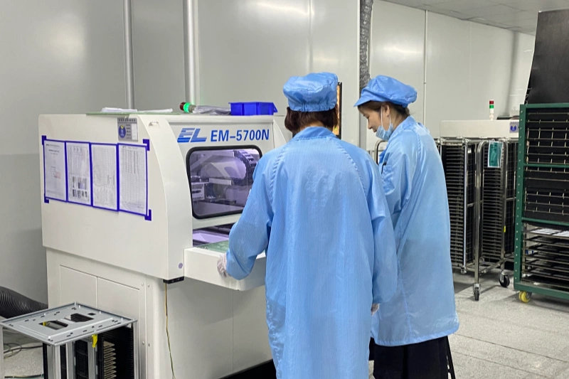
Before full production, prototypes must be checked to make sure all parts are connected and the board works.
What types of PCBs are there?
To meet a device’s design, use, and complexity, you must choose the right PCB type. The board can be rigid or flexible.
Rigid PCB
Built not to bend or change shape.
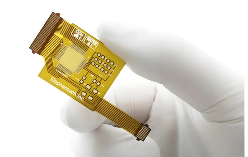
Flexible PCB
Can fold, twist, and bend to fit a shape. They are thinner, lighter, and can fit special forms.
Cost: flexible vs rigid
Rigid PCBs are usually cheaper to make in large runs because they are easy to mass produce with automated lines.
Flexible PCBs can remove the need for connectors and lower total production cost in some designs. But they need extra steps for part fixing and assembly automation, which can raise cost.
Cost is not the only factor. Weight, space, and design limits also affect the choice between rigid and flexible boards.
PCB layers explained
Single-layer PCB
One layer of conductive copper on one side of the base. These are simple and fast to produce.
Double-layer PCB
Copper on both sides of the board. You can use through-hole or surface mount parts.
Multi-layer PCB
Four layers or more for complex designs. Multi-layer boards save space and reduce wire harnesses, which lowers weight. They are ideal for aerospace, handheld devices, batteries, and many high-speed signal uses.
Why use a PCB?
PCBs give many benefits to engineers, OEMs, and designers, such as:
- Small space use — all connections are on the board so fewer wires are needed.
- Easier assembly and repair — parts are on the board and marked for simpler work.
- Faster assembly — PCBs speed up the build process vs loose wiring.
- Secure mounting and connection — parts are soldered to stay in place.
- Manufacturing efficiency — PCBs are cheaper for mass production.
- Reliable operation — soldered copper traces do not loosen like wires can.
What color is a PCB?
People often think the board color comes from the base, but it actually comes from the solder mask. Boards are commonly green, but the solder mask can be blue, yellow, orange, purple, red, black, white, or green.
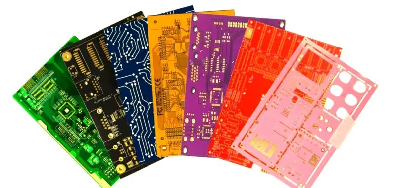
Does PCB color matter?
Color can matter for several reasons. It may match a brand, or it might help inspect boards. Some colors give better contrast for human inspection. White boards help reflect light and are useful when you need more light on the board, such as in LED lighting engines. White PCBs are often used in LED light systems.
In other uses, you may not want reflection. For example, DJ equipment used in dark clubs should not reflect light. The board color is one of the many decisions in the PCB design phase.
What is the PCB design process?
PCB manufacturing usually follows eight steps. Complexity varies by device design. The basic design steps are:
PCB design basics (short list)
- Device concept
- Create the schematic
- PCB layout design
- Final Bill of Materials (BOM)
- Make a PCB prototype
- Evaluate the prototype
- Install firmware / program the device
- Full production
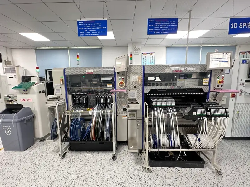
Production process steps
- PCB design
- Print copper on inner layers
- Remove extra copper (etching)
- Inspect and align layers
- Laminate layers together
- Drill holes
- Plate the board (copper plating)
- Meet RoHS and other compliance
How long does custom PCB design and production take?
Turnaround time depends on the supplier, the project size, and how complex the board is. From design to final product, a full PCB service can deliver in as little as four weeks for typical cases. Fast prototyping tools, like 3D printers and dedicated workspace, help teams speed up prototypes and the whole process.
Closing tips (simple)
- Start with a clear schematic and block layout. Place major parts first.
- Plan the layer stack-up early for high-speed or mixed-signal boards.
- Use proper decoupling, keep traces short, and match lengths for critical buses.
- Follow vendor notes for DDR, high-speed parts, and special interfaces.