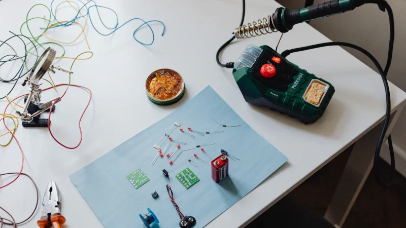
Through-Hole PCBs stand out as a straightforward solution for electronics project assembly, offering practical advantages that streamline the building process for hobbyists, developers, and small-scale producers alike.
Their components feature longer leads that insert directly through drilled holes in the board, making handling and manual assembly intuitive—no specialized skills or complex tools are required to position parts accurately. Soldering is equally hassle-free, with accessible connection points that reduce errors and cut down on assembly time, accelerating prototyping cycles and getting projects off the ground faster. Repairs and upgrades are simplified too: the robust lead connections allow for easy component removal and replacement, eliminating the frustration of dealing with delicate solder joints or damaged traces.
In addition to being easy of use, Through-Hole PCBs deliver reliable mechanical stability. The secure lead-to-board connections provide enhanced durability, making them ideal for high-power circuits, applications requiring frequent handling, or projects where long-term reliability is critical.
Key Points Summary
- Strong mechanical connections in Through-Hole PCBs provide durability, making them suitable for high-power circuits and environments with vibration.
- Using Through-Hole PCBs simplifies prototyping and testing, allowing for easy component swapping and adjustments during development.
- For reliable projects, choose Through-Hole PCBs in applications like automotive, medical devices, and industrial equipment where durability is crucial.
What Is a Through-Hole PCB?
Basic Definition
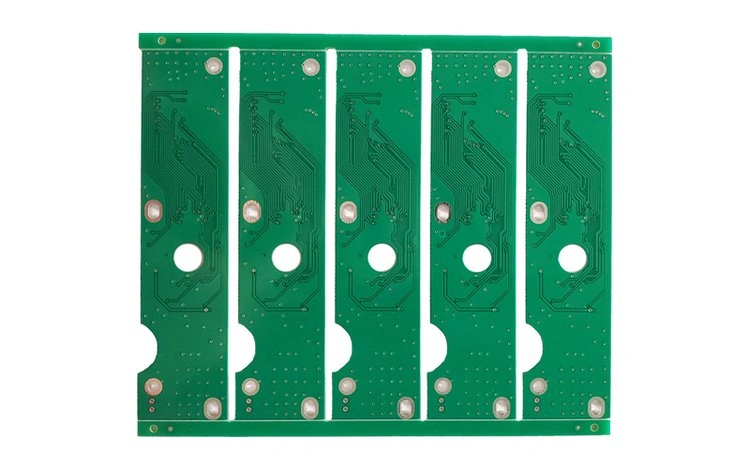
A Through-Hole PCB is a fundamental type of printed circuit board characterized by its simple, intuitive construction. Its core design involves drilling holes through the board, into which electrical connections leads are inserted. The leads are then soldered to the board’s conductive pads- creating secure, reliable electrical connections.
Through-Hole vs. Other PCB Types
When selecting a printed circuit board for a project, Through-Hole PCB and Surface-Mount Technology (SMT)PCBs, with distinct differences in their construction and assembly processes being the key differentiators. Here is the main features:
| Feature | Through-Hole PCB | Surface-Mount PCB |
| Component Insertion | Components with long leads inserted into plated holes | Components attach to the PCB surface without holes |
| Assembly Method | Typically hand-soldered, easier for hobbyists | Requires automated assembly, more complex |
| Component Density | Lower density, larger footprint | Higher density, smaller footprint |
| Prototyping | Easier for quick prototypes, can use larger components | More efficient for final production |
| Cost Efficiency | No need for solder stencils or pick-and-place setup | Higher initial setup costs but better for mass production |
| Testing | Manual in-house testing possible | Requires specialized fixtures for testing |
Through-Hole PCBs stand out for their user-friendly assembly, thanks to larger component sizes that are easier to handle during manual operations. In contrast, Surface-Mount PCBs (SMT) utilize significantly smaller components, which typically demand precision tools and steady handling. This complexity can pose notable challenges, especially for those new to electronics assembly.
A common pain point shared by beginners is the difficulty of manual assembly and rework with SMT PCBs. The minute size of SMT components complicates positioning and soldering, and repairs often require specialized tools. By eliminating these barriers, Through-Hole PCBs emerge as the preferred choice for educational purposes, prototyping, and any scenario where ease of use and mechanical durability are prioritized.
Why Through-Hole PCB Simplifies Projects
Easy Component Placement
Through-Hole PCBs excel in user-friendly component placement, thanks to their larger-sized components that are intuitive to grip, position, and align—even for those with limited assembly experience. No specialized tools or magnification equipment is required, as the distinct lead positions and clear board layout enable quick, accurate placement while minimizing errors.
- Through-hole components are durable and facilitate manual assembly, making them easier to place compared to other types of PCBs.
- They require careful planning for placement to ensure mechanical stability and ease of soldering.
- Adequate spacing around leads is necessary for manual soldering, which simplifies the assembly process.
The visible leads and ample spacing not only enhance assembly efficiency but also boost confidence in build process, making Through- Hole PCBs particularly well-suited for educational settings and first-time project implementations.
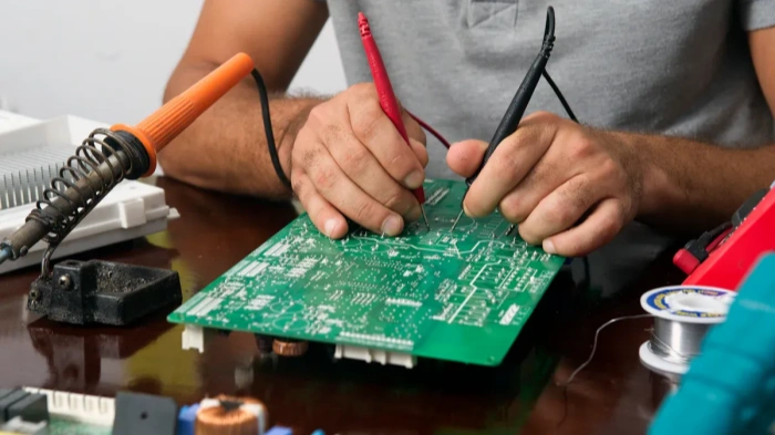
Simple Soldering and Repairs
Soldering on a Through-Hole PCBs is remarkably straightforward, attributed to the larger pads and component leads that provide ample surface area for solder application—eliminating the risk of board damage during the process. The forgiving nature of this design allows for easy component removal and replacement in case of errors, without compromising the integrity of surrounding circuitry.
- Larger components are easier to handle.
- The clear placement of leads helps in understanding circuit connections.
- Soldering through-hole parts is more forgiving, allowing for mistakes without damage.
Repairs and upgrades are equally efficient: visible connections make it easy to identify common issues like cold joints or solder bridges. Rework can be completed quickly, which is invaluable during prototyping phases or when time-sensitive adjustments are needed.
Strong Mechanical Connections
Mechanical strength stands out as a key advantage of Through-Hole PCB. The leads pass through the board and anchor securely with solder, creating robust connections that withstand physical stress.
Through-hole PCB connections provide strong mechanical bonds that are essential for enduring physical stress and environmental challenges. This durability is particularly crucial in high-reliability applications, ensuring that prototype devices can withstand vibration, thermal cycling, and other stresses, thereby enhancing their longevity.
Practical Uses of Through-Hole PCB
Prototyping and Testing
Through-Hole PCBs are a trusted solution for electronics prototyping and testing, thanks to their design that enables effortless component placement, soldering, and swapping. This inherent flexibility accelerates the development cycle, allowing designers to refine concepts efficiently before transitioning to mass production.
Widely favored by engineers and hobbyists for rapid prototyping, Through-Hole PCBs simplify hand soldering, enabling quick circuit revisions and hassle-free component replacement. This ease of adjustment makes it straightforward to test multiple design configurations, while the mechanical robustness of through-hole mounting ensures prototypes can withstand repeated handling and operational stress, delivering reliable performance throughout the testing phase.
Tip: Opt for Through-Hole PCBs when testing high-power circuits or devices exposed to vibration. The sturdy connections reduce the risk of failure during experiments.
Through-hole PCBs used in many industries for prototyping and testing. Here are some common applications:
- Military and aerospace devices must resist harsh conditions and mechanical loads.
- Automotive electronics endure vibrations and thermal cycling.
- Industrial machinery handles higher power demands in tough environments.
- Consumer electronics, such as household appliances, require mechanical stability.
- Medical devices, including heart pacemakers, demand consistent performance.
- Power supplies and converters need to handle significant current and voltage.
- Test and measurement equipment benefits from durability and easy maintenance.
When comparing Through-hole and surface-mount PCBs, distinct advantages of Through-Hole technology for prototyping become evident:
| Type | Advantages | Disadvantages |
| Surface-Mount | Smaller components, higher density | Harder to repair manually, requires precise machinery |
| Through-Hole | Easier for prototyping, more durable | Bulky, less suitable for automated assembly |
Through-Hole PCBs are highly favored for early-stage development, as they support circuit testing, repair, and modification without the need for specialized tools. This streamlined approach optimizes development timelines and mitigates operational inefficiencies.
When to Choose Through-Hole PCB
Ideal Scenarios
Through-Hole PCBs are a preferred selection for projects requiring enhanced reliability and structural strength. Given that specific environments and applications demand robust electrical connections paired with convenient repairability, the following scenarios are deemed ideal for this technology:
- Automotive electronics, such as engine control units and safety systems, where vibration and temperature changes are common.
- Industrial equipment, including power supplies, controllers, and inverters, which require strong connections and good heat dissipation.
- Medical devices, like diagnostic equipment and implantable electronics, where accuracy and long-term reliability matter most.
- Power circuits and connectors that handle high currents and voltages, ensuring stability and safety.
- Prototyping and testing boards, where I need to swap components and make adjustments quickly.
These situations benefit from the mechanical durability and straightforward assembly that through-hole technology provides.
Tips for Selection
Choosing the right PCB type for a project requires evaluating key factors:
| Decision Factor | Through-Hole PCBs (THT) | Surface-Mount PCBs (SMT) |
| Mechanical Durability | High, suitable for rugged use | Lower, best for compact designs |
| Heat Dissipation | Better, larger thermal mass | May need extra thermal management |
| Manufacturability | Slower for large runs | Faster, ideal for mass production |
| Production Size | Best for small-scale or prototyping | Preferred for large-scale production |
| Application Suitability | Ideal for high-power circuits | Suited for low-power, compact devices |
Here also some best practices to avoid common mistakes:
- Maintain at least 100mil clearance around hole pads to prevent shorts.
- Avoid routing traces near non-plated through holes.
- Use teardrop pads to reduce stress on solder joints.
- Check hole and pad diameter ratios before starting assembly.
Tip: Before finalizing the layout, run a Design Rule Check (DRC) and label all components. This pre-production step helps identify errors at an early stage, guaranteeing a smooth assembly workflow.
By considering these factors and following these tips, to make sure projects benefit from the strengths of through-hole technology.
For electronics projects and educational initiatives, Through-Hole PCBs stand out for their simplicity and reliability. Their core strengths include:
- Strong mechanical bonds for durability in harsh environments.
- Easy manual soldering and repairs, perfect for hands-on learning.
- Flexibility for prototyping and quick modifications.
FAQ
What essential tools need to assemble a through-hole PCB?
A soldering iron, solder wire, wire cutters, and tweezers and a multimeter for check connections. plus an optional desoldering pump for repairs. These basic tools cover most assembly and troubleshooting needs.
Can components from a through-hole PCB be reused?
Yes, through-hole components are reusable. Simply heat the solder joints to melt the solder, then gently remove the parts. It’s recommended to inspect each component for damage before integrating it into a new project.
Are through-hole PCBs suitable for high-frequency circuits?
Through-hole PCBs are generally not ideal for high-frequency designs. Their longer component leads tend to introduce unwanted inductance, which can impact performance. For high-speed or RF circuits, surface-mount technology (SMT) is typically preferred.
How fix a mistake on a through-hole PCB?
Fix mistakes by using a desoldering pump or braid to remove solder, carefully lifting and replacing the component, and inspecting the pad and trace for damage before resoldering.